Display device and a method of manufacturing the same

a display device and a manufacturing method technology, applied in the direction of electrical apparatus construction details, instruments, optics, etc., can solve the problems of increasing the cost due to a number of cofs, and achieve the effect of increasing the adhesive strength between the driving film and the array substrate, increasing the reliability of the display device, and increasing the adhesive strength

Inactive Publication Date: 2012-10-11
SAMSUNG DISPLAY CO LTD
View PDF4 Cites 14 Cited by
  • Summary
  • Abstract
  • Description
  • Claims
  • Application Information

AI Technical Summary

Benefits of technology

[0029]According to a display device and a method of manufacturing the same of example embodiments of the present invention, a dummy pad is formed on the array substrate, and the dummy pad adheres to an alignment mark of the driving film, so that the driving film is prevented from separating from the array substrate. Thus, the reliability of the display device may be increased.
[0030]In addition, when signal pads are formed on the array substrate, a dummy pad may be simultaneously formed on the array substrate. Thus, the adhesive strength between the driving film and the array substrate may be increased without adding another process.

Problems solved by technology

For example, when the driving part is formed in the COF type, eight COFs to fourteen COFs may be used, and then a cost may be increased due to a number of the COFs.

Method used


Image

  • Display device and a method of manufacturing the same
  • Display device and a method of manufacturing the same
  • Display device and a method of manufacturing the same

Examples


Embodiment Construction

[0040]Hereinafter, exemplary embodiments of the present invention will be explained in detail with reference to the accompanying drawings.

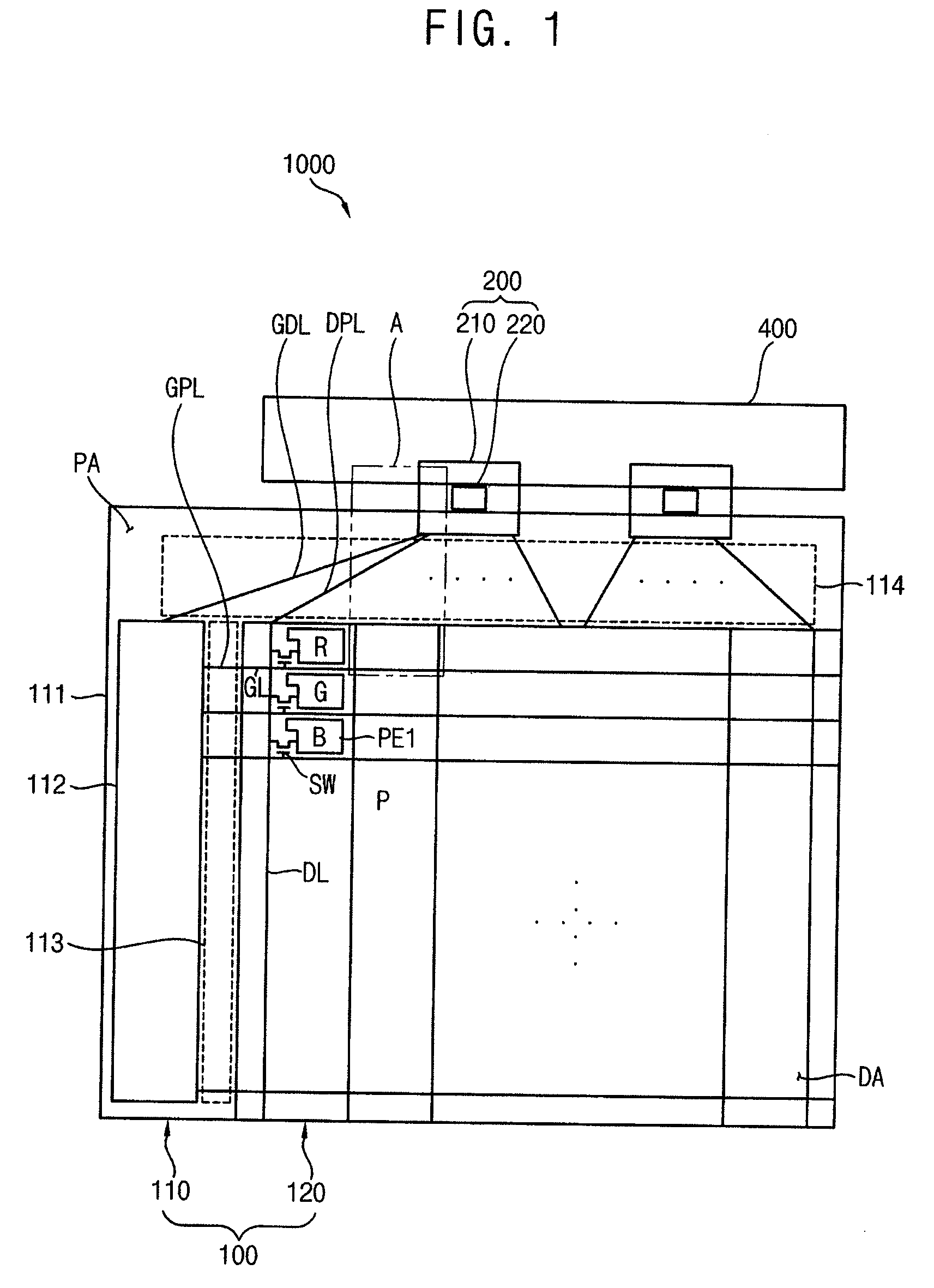
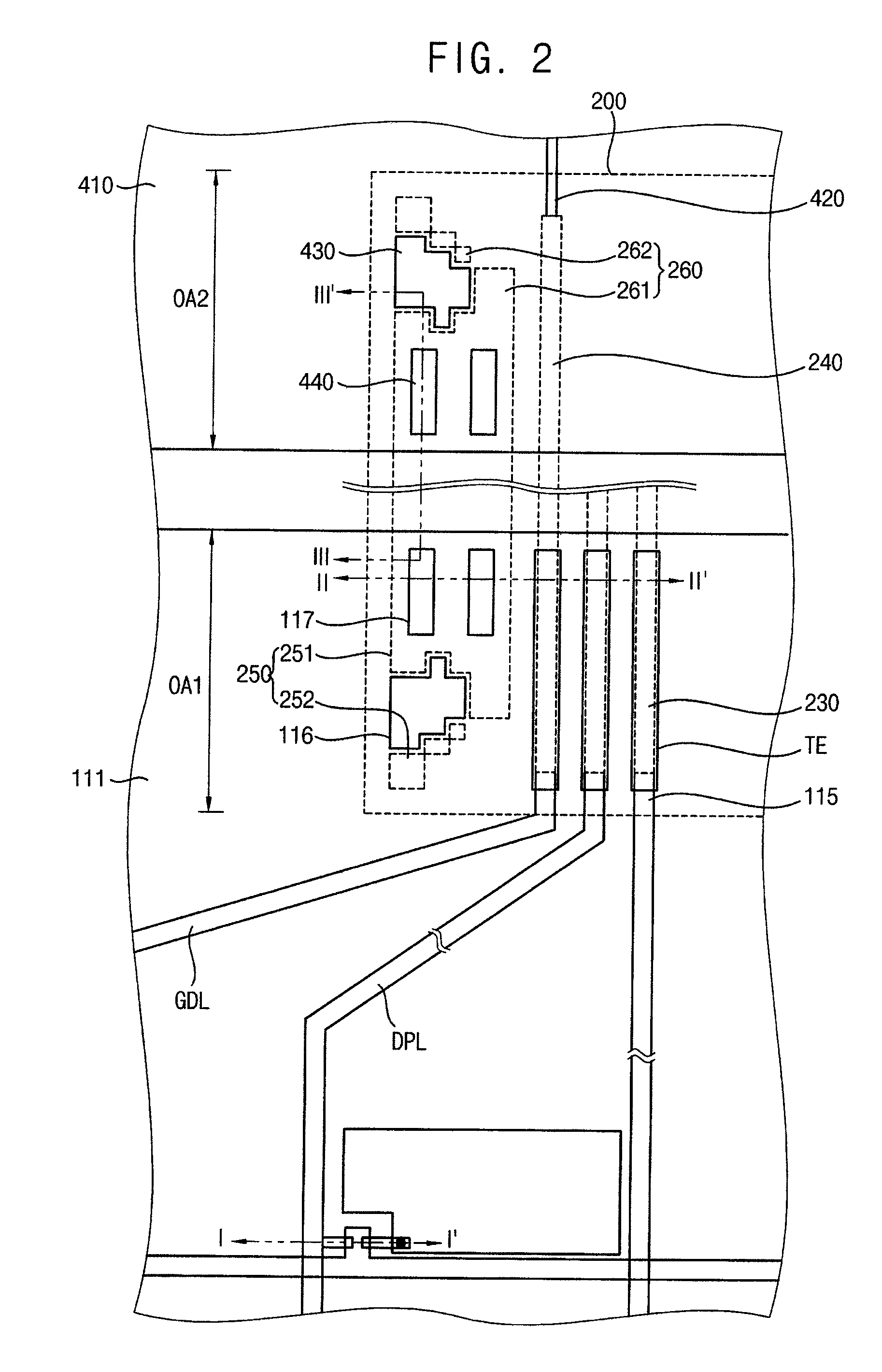
[0041]FIG. 1 is a plan view illustrating a display device according to an example embodiment of the present invention. FIG. 2 is an exploded plan view of ‘A’ portion of FIG. 1.

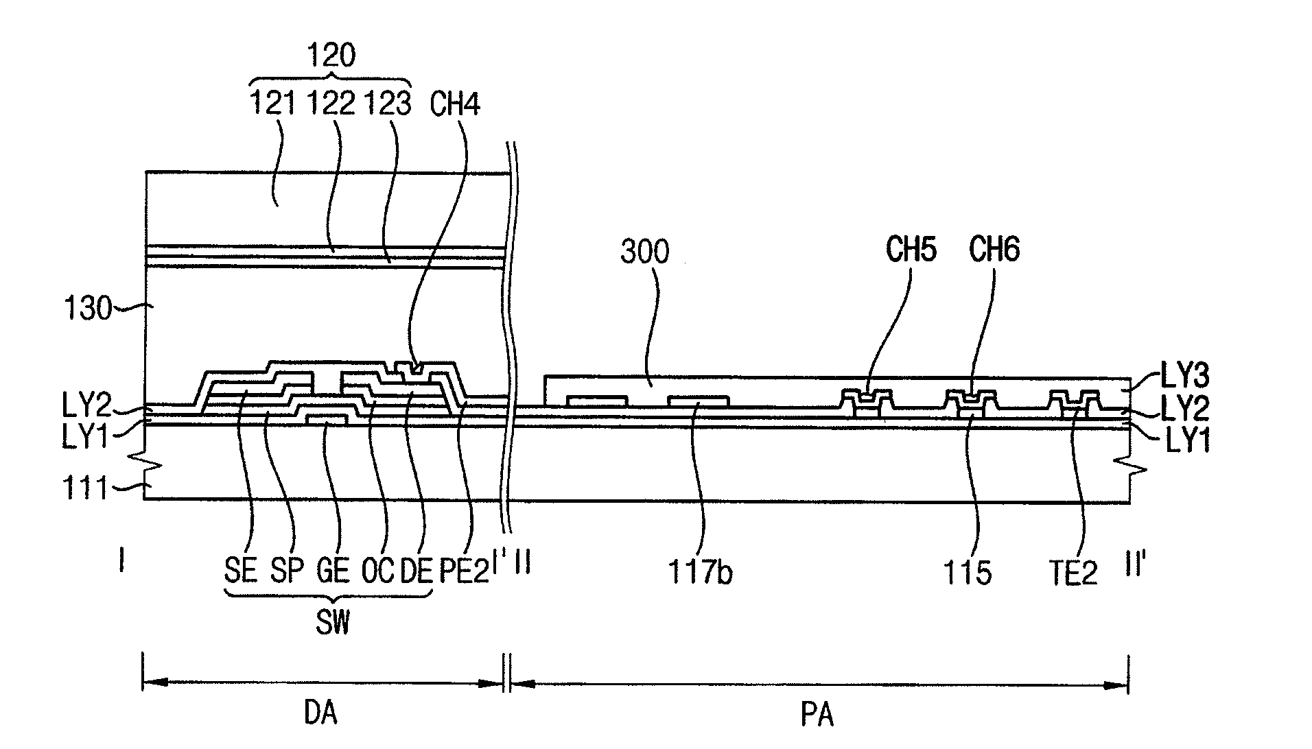
[0042]Referring to FIGS. 1 and 2, a display device 1000 includes, for example, a display panel 100, a driving film 200 and an adhesive member 300. The display device 1000 may further include a print circuit board (PCB) 400. The display panel 100 includes an array substrate 110, an opposite substrate 120 facing to the array substrate 110 and a liquid crystal layer (not shown) between the array substrate 110 and the opposite substrate 120.

[0043]The array substrate 110 is divided into a display area DA overlapping the opposite substrate 120 and displaying an image and a peripheral area PA surrounding the display area DA. The array substrate 110 includes, for example, a first ba...


PUM


Abstract

A display device includes an array substrate, a driving film and an adhesive member. The array substrate includes a first base substrate, a plurality of first signal pads formed on the first base substrate and a first dummy pad formed adjacent to the first signal pads. The driving film includes a base film, a plurality of output terminals formed on the base film and a first alignment mark formed adjacent to the output terminals. The adhesive member adheres the first signal pads to the output terminals, and adheres the first dummy pad to the first alignment mark.

Description

CROSS-REFERENCE TO RELATED APPLICATION[0001]This application claims priority under 35 U.S.C. §119 to Korean Patent Application No. 2011-0031971, filed on Apr. 7, 2011, the disclosure of which is hereby incorporated by reference herein in its entirety.BACKGROUND OF THE INVENTION[0002]1. Technical Field[0003]Example embodiments of the present invention relate to a display device and a method of manufacturing the display device. More particularly, example embodiments of the present invention relates to a display device including a flat display panel and a method of manufacturing the display device.[0004]2. Description of the Related Art[0005]A display device may include a display pane, a driving part and a printed circuit board (PCB). The display panel includes an array substrate including a plurality of data lines and a plurality of gate lines crossing the data lines formed on a substrate and an opposite substrate positioned opposite to the array substrate. The driving part drives the...

Claims


Application Information

Patent Timeline
Patent Type & Authority Applications(United States)
IPC IPC(8): H01L33/08
CPCG02F1/13452G02F1/1345
Inventor LEE, JAE-HANLEE, JONG-MINSON, SUN-KYUBAN, YOUNG-ILSHIN, OK-KWON
Owner SAMSUNG DISPLAY CO LTD
Why Eureka
Try Eureka