

Display device
- Summary
- Abstract
- Description
- Claims
- Application Information
AI Technical Summary
Benefits of technology
Problems solved by technology
Method used
Image

Examples
embodiment modes
[0065]Hereinafter, embodiment modes will be described with reference to the drawings. Note that the embodiment modes are not limited to the following description, and it is easily understood by those skilled in the art that the modes and details disclosed herein can be modified in various ways without departing from the spirit and scope of the embodiment modes. Thus, the embodiment modes should not be taken as being limited to the following description of the embodiment modes. Note that the same reference numeral is commonly used to denote the same component among the different drawings in the structure of the embodiment modes described below.
embodiment mode 1
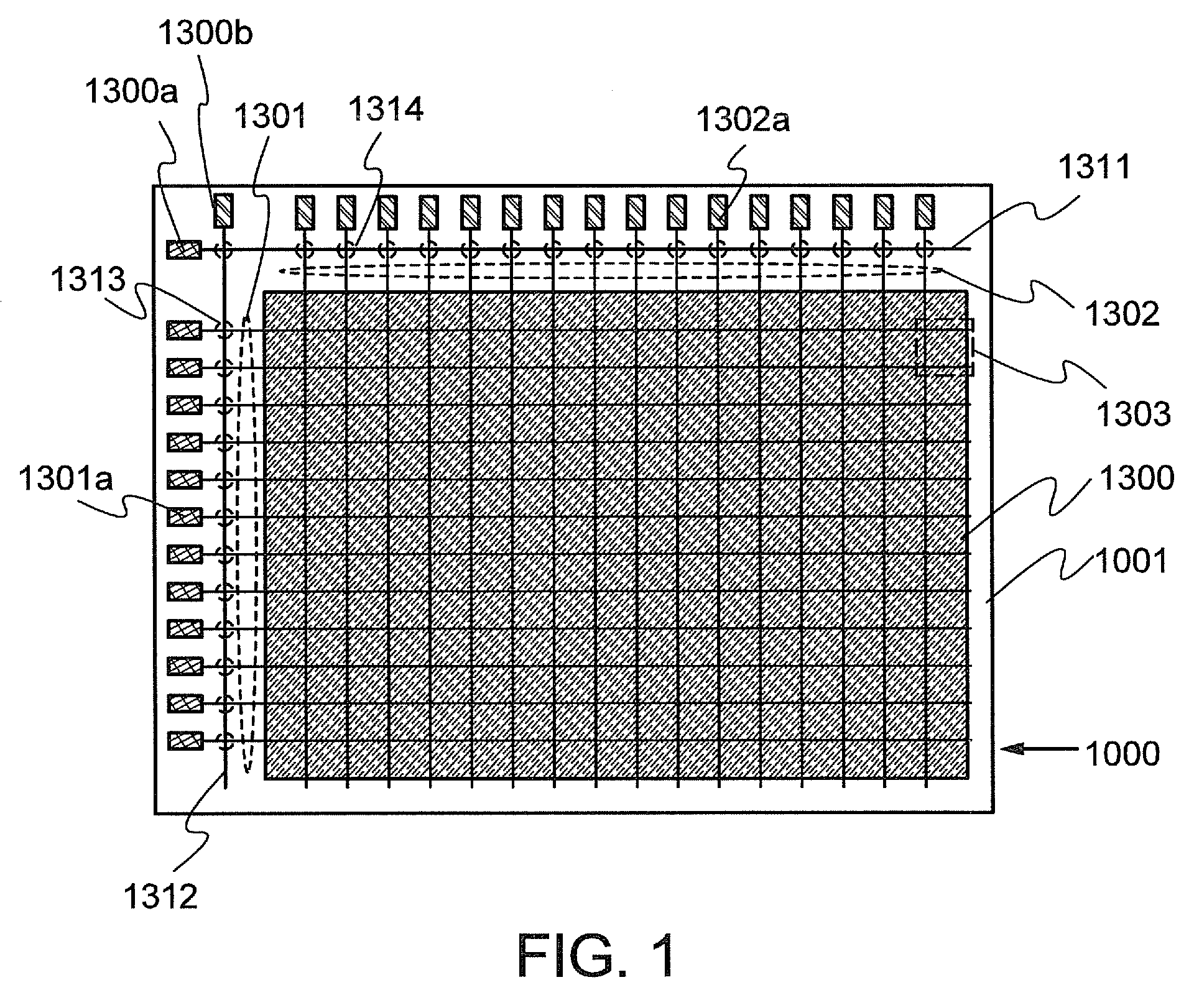
[0066]Here, a structure of a protection circuit is described. Note that in an element substrate 1000 illustrated in FIG. 1, a plurality of first wirings which extends in a first direction and is lined up in a second direction intersecting the first direction is referred to as scan lines, while a plurality of second wirings which extends in the second direction and is lined up in the first direction is referred to as signal lines. In a pixel provided in a pixel portion, the scan line is connected to a gate electrode in the case of an active matrix display device provided with a switching element that controls potential of a pixel electrode. Alternatively, part of the scan line functions as a gate electrode. Therefore, the first wiring is referred to as a gate wiring 1301 hereinafter. In addition, since the signal line is connected to a source of the switching element, the second wiring is referred to as a source wiring 1302 hereinafter. However, when the second wiring is connected to...
embodiment mode 2
[0090]In this embodiment mode, a method of manufacturing the protection circuit illustrated in FIGS. 2A and 2B and FIGS. 4A to 4D described in Embodiment Mode 1 will be described with reference to FIGS. 5A to 5D and FIGS. 6A to 6D.
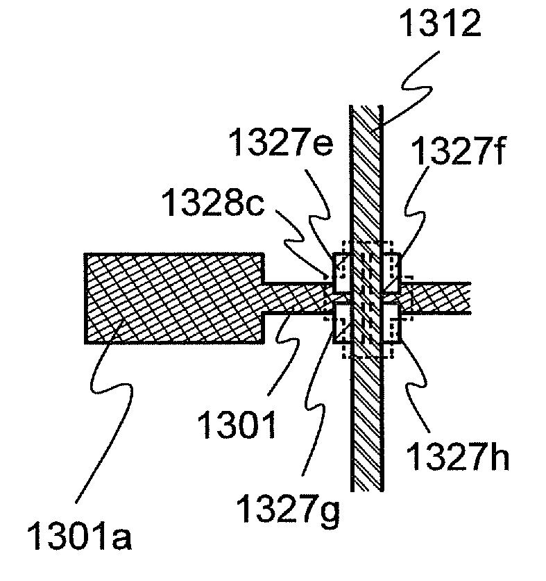
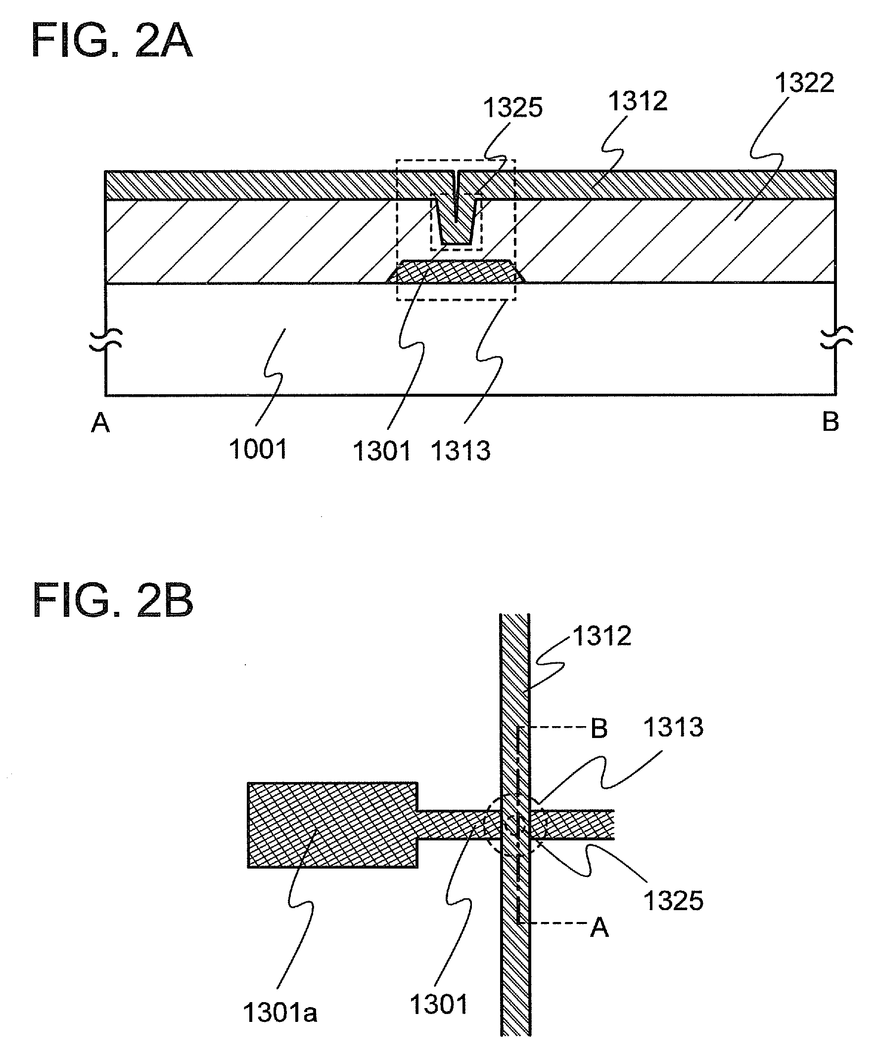
[0091]FIG. 5D is a plan view at the intersection of the gate wiring 1301 and the second common line 1312, and FIG. 5C illustrates a cross-sectional view taken along line A-B of FIG. 5D.
[0092]As illustrated in FIG. 5A, the gate wiring 1301 is formed over the substrate 1001. Next, the first insulating film 1323 is formed over the gate wiring 1301. Then, the second insulating film 1324 is formed over the first insulating film 1323. The first insulating film 1323 and the second insulating film 1324 may be formed using an insulating material, as appropriate. However, it is preferable that a combination in which only the second insulating film 1324 can be selectively etched be used. For example, the first insulating film 1323 is formed using an inorganic insulat...
PUM
 Abstract
Description
Claims
Application Information