Transmitter circuit

Inactive Publication Date: 2012-07-26
HITACHI LTD
View PDF8 Cites 8 Cited by
  • Summary
  • Abstract
  • Description
  • Claims
  • Application Information

AI Technical Summary

Benefits of technology

[0008]Accordingly, the present invention is a transmitter circuit system devices as a countermeasure of the above-explained situation and a preferred aim of the present invention is to provide a transmitter circuit that is advantageous in the two points, that is, elimination of correction circuits and reduction in occupying area of element circuits and capable of resolving the unbalance of emphasis amount on the High side and Low side of output level.
[0017]That is, in a transmitter circuit, it is possible to eliminate correction circuits and reduce an occupying area of element circuits and thus unbalance in the emphasis amounts on High side and Low side of an output level without level correction can be resolved upon level output of three-valued or more. As a result, an occupying area of the transmitter circuit can be reduced more than existing transmitter circuits and thus downsizing of the chip size can be achieved.

Problems solved by technology

However, in the CML system, when the supply voltage is low, the MOS transistor of the current source operates in the linear region and thus output current for determining the level is insufficient; therefore, the level on the Low side is increased more than a desired level and an unbalance may occur in the emphasis amounts on the High side and Low side.

Method used


Image

  • Transmitter circuit
  • Transmitter circuit
  • Transmitter circuit

Examples


first embodiment

[0046]A first embodiment of the present invention will be described hereinafter with reference to FIGs. 1 to 5. A transmitter circuit according to the first embodiment is an example of a type not separating the waveform-equalizing function and the load-driving function.

[0047]

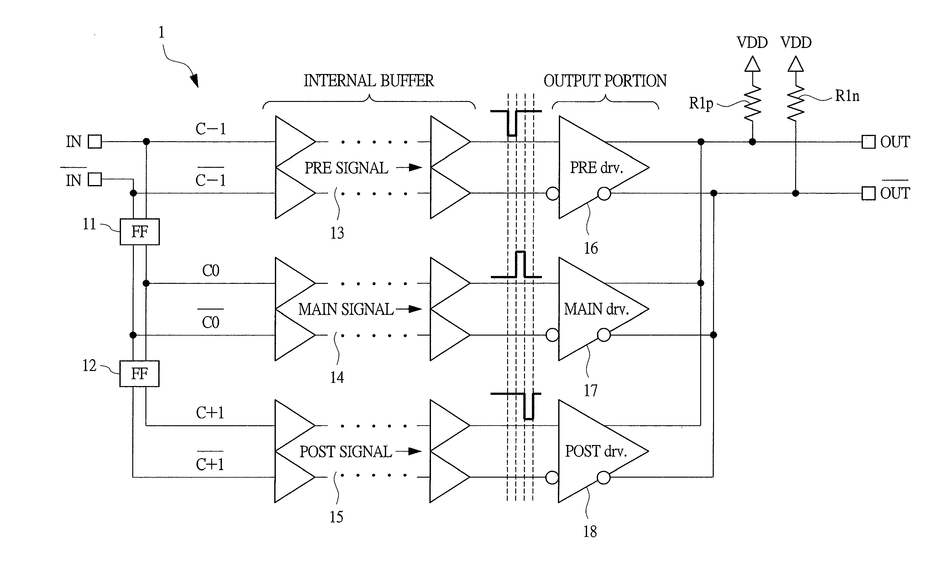
[0048]First, a configuration of a transmitter circuit according to a first embodiment will be described with reference to FIG. 1. FIG. 1 is a diagram illustrating an example of a configuration of the transmitter circuit.

[0049]A transmitter circuit 1 of the first embodiment includes: two flip-flop circuits 11 and 12; three buffer circuits 13, 14, and 15 as internal buffers; three driver circuits 16 (PRE drv.), 17 (MAIN dry.), and 18 (POST dry.) as output portions; and load resistors R1p and R1n, etc. Differential transmitted data signals are inputted to input terminals (In, / IN) and then waveform-equalized, and further signal-amplified and then outputted as differential transmitted data signals to output terminal...

second embodiment

[0083]A second embodiment of the present invention will be described with reference to FIGs. 6 to 8. A transmitter circuit according to the second embodiment is different from that of the first embodiment in a point that the second embodiment is an example of a type having the waveform-equalizing function and the load-driving function separated. In the second embodiment, the difference from the first embodiment will be mainly described and descriptions of identical portions will be omitted.

[0084]

[0085]First, a configuration and operations of a transmitter circuit of the second embodiment will be described with reference to FIG. 6. FIG. 6 is a diagram illustrating an example of a configuration of the transmitter circuit.

[0086]A transmitter circuit 2 of the second embodiment is configured by two flip-flop circuits 11 and 12, three buffer circuits 13, 14 and 15, three driver circuits 16 (PRE dry.), 17 (MAIN dry.) and 18 (POST dry.), load resistors R1p and R1n, a load driver circuit 21,...


PUM


Abstract

A transmitter circuit in which a driver circuit includes MOS transistors for bias voltage application, in which a driving current flows, cascode-connected to MOS transistors for differential signal input controlled by a voltage value of transmitted data signals, controlled by a voltage value of a bias voltage, and driver circuits include MOS transistors for bias voltage application, in which a driving current flows, cascode-connected to MOS transistors for differential signal input that is controlled by a voltage value of signals obtained by the transmitted data signals, connected to a load portion, and controlled by a voltage value of a bias voltage.

Description

CROSS-REFERENCE TO RELATED APPLICATION[0001]The present application claims priority from Japanese Patent Application No. 2011-013795 filed on Jan. 26, 2011, the content of which is hereby incorporated by reference into this application.TECHNICAL FIELD OF THE INVENTION[0002]The present invention relates to technology of a transmitter circuit. More particularly, the present invention relates to technology effectively applied to a transmitter circuit provided to a data transmitting system that transmits data to a receiver circuit via transmission paths from the transmitter circuit.BACKGROUND OF THE INVENTION[0003]There are examples of technology related to a transmitter circuit provided to a data transmitting system which transmits data to a receiver circuit via transmission paths from the transmitter circuit described in U.S. Pat. No. 7,180,333 (Patent Document 1), U.S. Pat. No. 6,977,525 (Patent Document 2), International Patent Application Publication No. WO2002 / 039684 (Patent Docum...

Claims


Application Information

Patent Timeline
IPC IPC(8): H03K19/0185H03K19/0175
CPCH03K19/018514
Inventor KURAHASHI, HIROAKIHOKARI, TOMOFUMIMUTO, TAKASHIONO, GOICHIYAMASHITA, HIROKI
Owner HITACHI LTD
Why Eureka
Try Eureka