Multilayer printed wiring board and method of measuring characteristic impedance

Inactive Publication Date: 2007-09-27
NEC CORP
View PDF3 Cites 8 Cited by
  • Summary
  • Abstract
  • Description
  • Claims
  • Application Information

AI Technical Summary

Benefits of technology

[0013]With the multilayer printed wiring board according to the first aspect of the present invention, and the method of measuring characteristic impedance according to the present invention, the test coupons for measuring characteristic impedance of the respective signal wiring layers are serially connected via through holes, which makes it possible to apply a step pulse to the respective test coupons at a time and to thereby efficiently measure the characteri

Problems solved by technology

In an electronic circuit element operating at high speed, a reflection wave caused by impedance mismatching becomes a cause of generating a trouble in the operation of the electronic circuit element.
However, in the case where the test coupon as shown in FIG. 6 is formed, the occupied area of the test coupon becomes large, which often results in a situation where the area required for the test coupon cannot be secured on the wiring board.
However, in this technique, the characteristic impedance of a signal wirin

Method used


Image

  • Multilayer printed wiring board and method of measuring characteristic impedance
  • Multilayer printed wiring board and method of measuring characteristic impedance
  • Multilayer printed wiring board and method of measuring characteristic impedance

Examples


Example

[0024]In the following, an exemplary embodiment according to the present invention will be described with reference to the accompanying drawings.

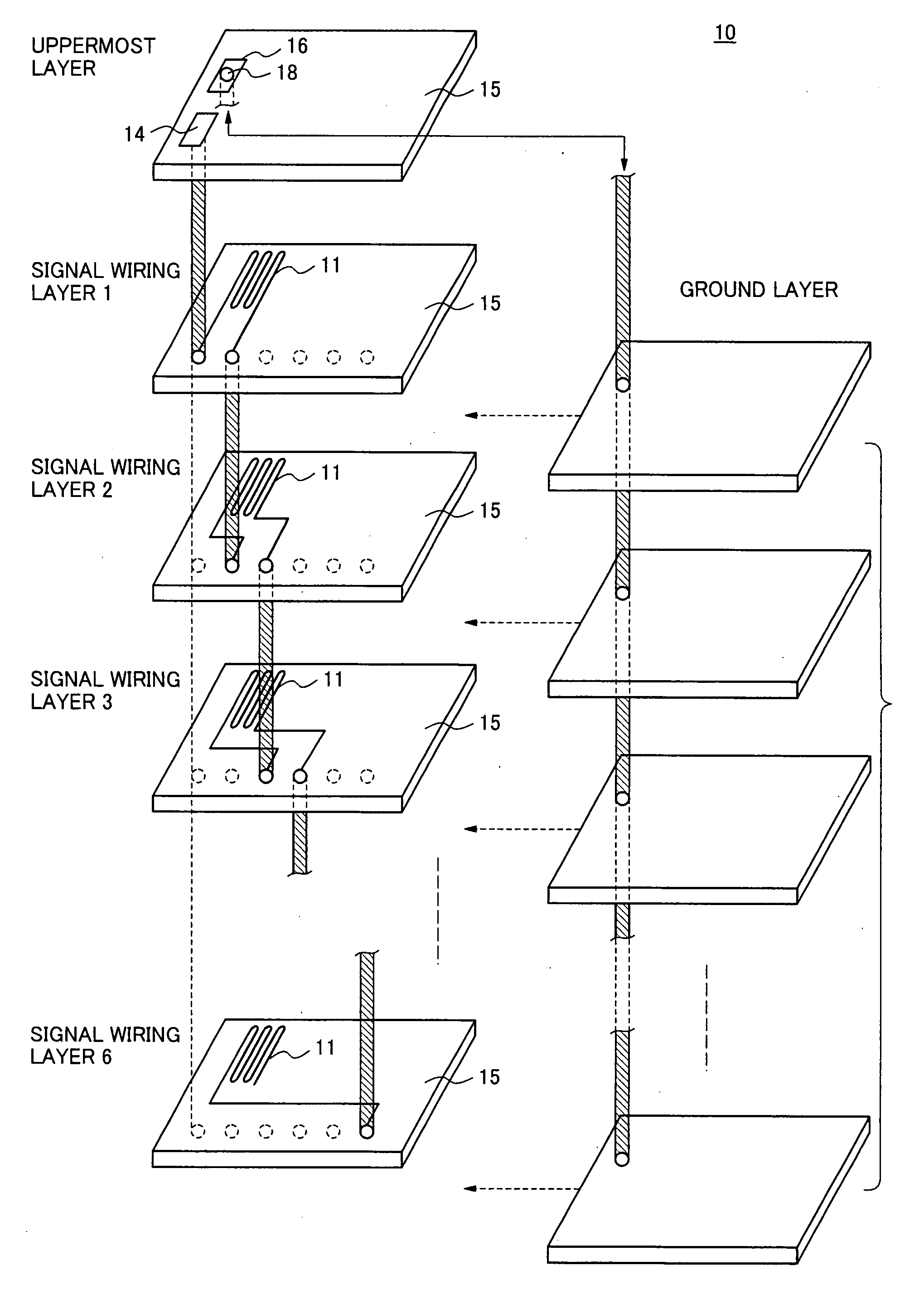
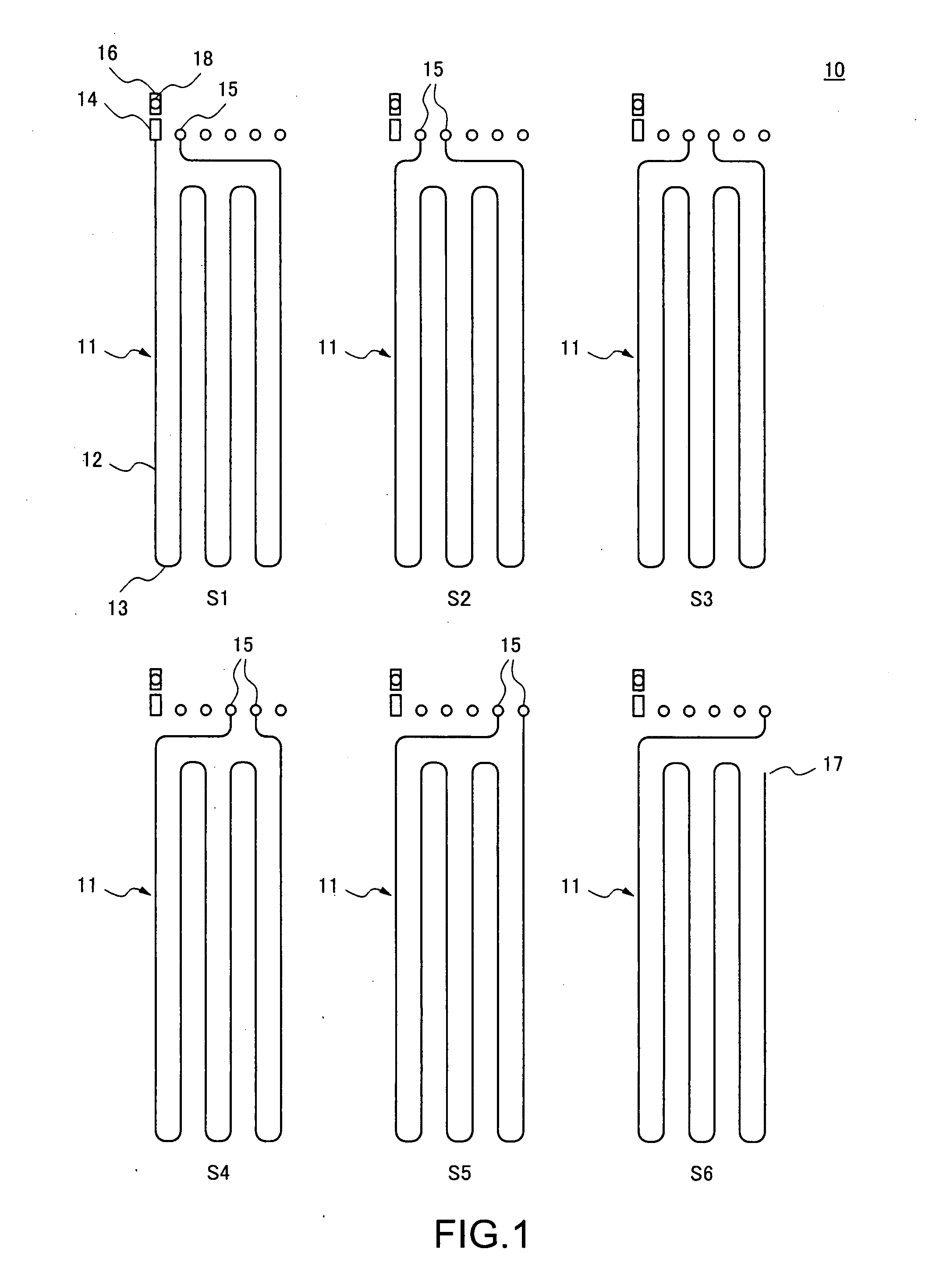
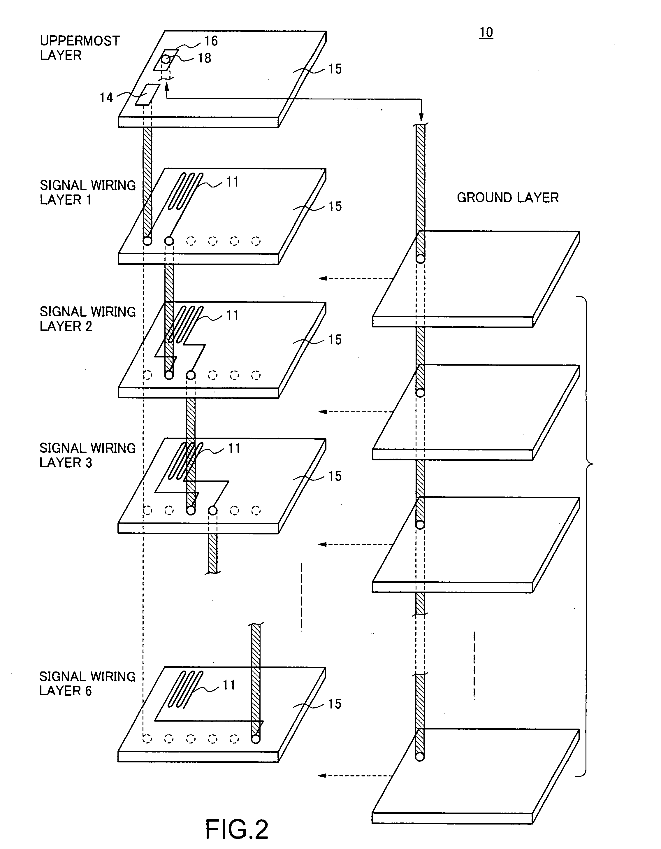
[0025]FIG. 1 is a plan view showing a wiring pattern of a test coupon formed on each signal wiring layer in a multilayer printed wiring board 10 according to an embodiment of the present invention. Further, FIG. 2 is an exploded perspective view schematically showing the multilayer printed wiring board 10 according to the embodiment of the present invention.

[0026]Each test coupon formed on a multilayer printed wiring board 10 is constituted by an individual test coupon (pattern wiring part) 11 formed on a wiring board of each signal wiring layer, and through holes 15 which mutually connects the pattern wiring parts 11 of the respective signal wiring layers. The pattern wiring part 11 is extended from the connecting part with the through hole 15, and constituted by six linear parts 12 each of which has a width of 0.08 mm to 0.3 mm and a leng...


PUM


Abstract

A multilayer printed wiring board having a compact test coupon formed on each of the signal wiring layers is provided, and accurate and efficient method of characteristic impedance measurement for each signal wiring layer is realized. The test coupon is constituted by a plurality of linear parts extending parallel to each other and folded-back parts mutually connecting the linear parts. A through hole is provided for serially connecting the respective test coupons of the signal wiring layers adjoining each other. Two measuring pads, one is connected to one end of the serially connected test coupons and another is connected to the ground layer, are also provided. The measurement is performed by applying a step pulse between two measuring pads and measuring voltages of reflection waves from the serially connected test coupons.

Description

BACKGROUND OF THE INVENTION[0001]1. Field of the Invention[0002]The present invention relates to a multilayer printed wiring board on which electronic circuit elements are mounted, and to a method of measuring characteristic impedance of signal wirings formed on the multilayer printed wiring board. More particularly, the present invention relates to a technique for measuring characteristic impedance of signal wirings of a multilayer printed wiring board by using a TDR (Time domain Reflectometry) method.[0003]2. Description of the Related Art[0004]In recent years, along with the increase of demand in the density of printed wiring boards, there has been used a multilayer printed wiring board formed by laminating wiring boards, each of which has a wiring pattern formed thereon, in three layers or more including the surface wiring board layer. Further, the operating speed of electronic circuit elements mounted on the multilayer printed wiring board has been more and more increased. In a...

Claims


Application Information

Patent Timeline
IPC IPC(8): G01R31/26
CPCG01R31/2818H05K1/0237H05K2201/09263H05K3/429H05K3/4611H05K1/0268G01R31/2813
Inventor ETO, JUN
Owner NEC CORP
Why Eureka
Try Eureka