
Display substrate and method of manufacturing the same

a technology of display substrate and manufacturing method, which is applied in the direction of electrical equipment, semiconductor devices, instruments, etc., can solve the problems of signal delay generation, limited process control ability, and inability to manufacture a display substrate by controlling a process so as to not change an inherent property of low resistance metal such as aluminum (al), copper (cu), etc., so as to reduce the resistance of signal lines and enhance the manufacturing reliability of patterns formed in the following process.

Active Publication Date: 2013-01-22
SAMSUNG DISPLAY CO LTD
View PDF1 Cites 4 Cited by
  • Summary
  • Abstract
  • Description
  • Claims
  • Application Information

AI Technical Summary

Benefits of technology

[0020]According to a display substrate and a method of manufacturing the display substrate, a signal line is formed in a trench formed by using a planarization layer and an insulation substrate, so that a resistance of the signal line may be reduced.
[0021]Moreover, the trench is formed through the planarization layer and in the insulation substrate via a dry-etching process, so that the trench may be formed in the display substrate in a stable structure. The signal line is formed by using a metal paste and a surface of the signal line is polished to have a plan surface, so that a manufacturing reliability of patterns formed in a following process may be enhanced.

Problems solved by technology

As LCD panels become larger and higher resolutions are required, lengths of the gate lines and the data lines become long, so that a signal delay is generated.
However, the types of the low resistance metal are limited.
In addition, the ability to manufacture a display substrate by controlling a process so as to not change an inherent property of the low resistance metal such as aluminum (Al), copper (Cu), etc is limited.
Moreover, when a thickness of a gate pattern including the gate line is increased, as a result of a step difference between the gate pattern and the base substrate, data patterns formed after the gate pattern is formed are easily cut at a side wall of the gate pattern, which can cause a short.

Method used


Image

  • Display substrate and method of manufacturing the same
  • Display substrate and method of manufacturing the same
  • Display substrate and method of manufacturing the same

Examples

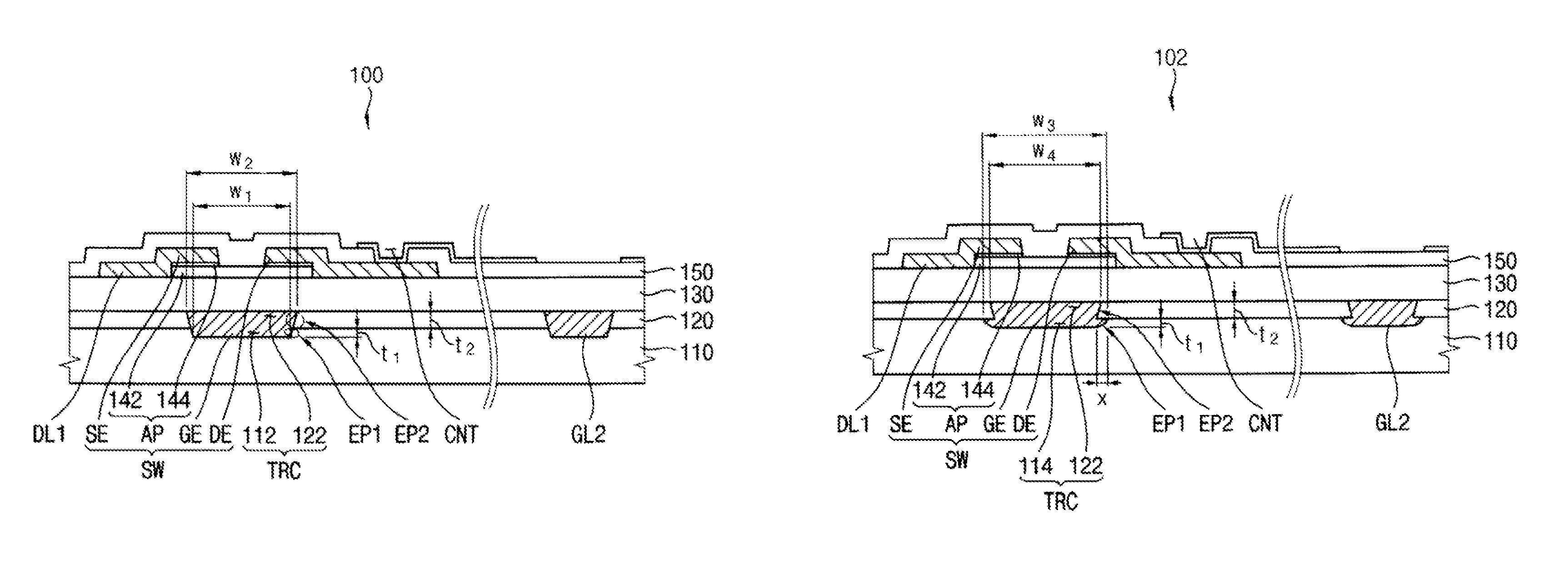
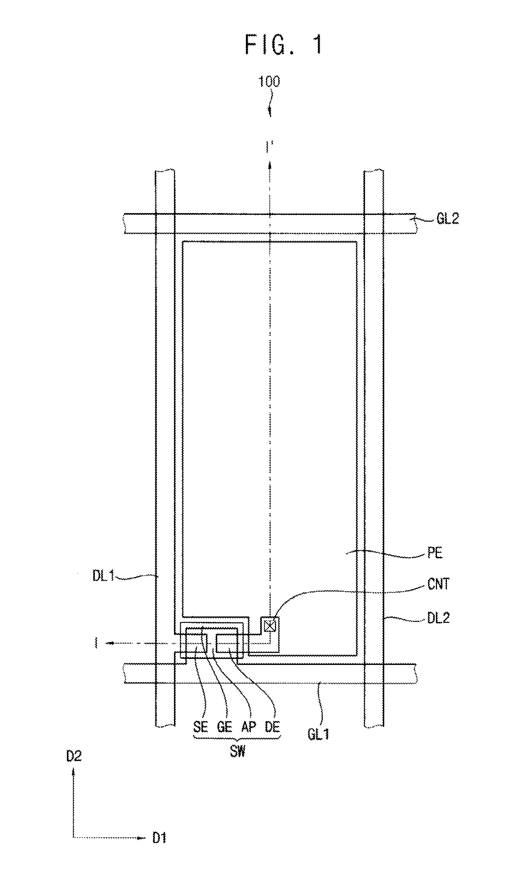
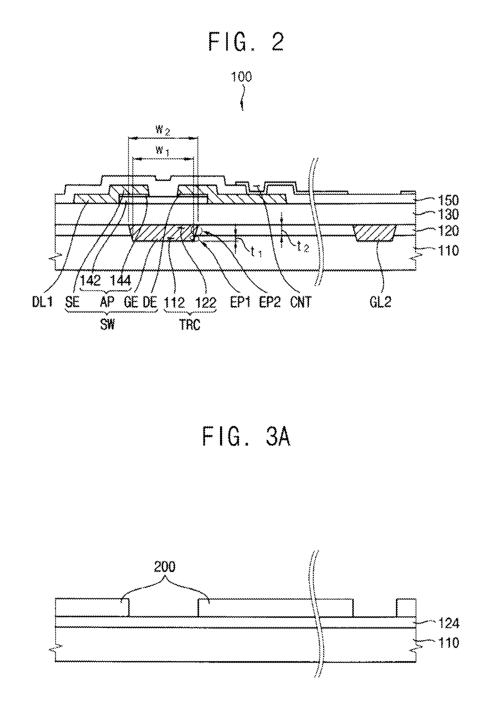

Embodiment Construction

[0029]Hereinafter, the exemplary embodiments will be explained in detail with reference to the accompanying drawings.

[0030]FIG. 1 is a plan view illustrating a display substrate according to one exemplary embodiment.

[0031]FIG. 2 is a cross-sectional view taken along a line I-I′ of FIG. 1.

[0032]Referring to FIGS. 1 and 2, a display substrate 100 according to the present exemplary embodiment includes an insulation substrate 110, a first gate line GL1, a second gate line GL2, a first data line DL1, a second data line DL2, a thin-film transistor SW that is a switching element and a pixel electrode PE. The display substrate 100 may further include a gate insulation layer 130 and a passivation layer 150.

[0033]The insulation substrate 110 may include an optically transparent material. For example, the insulation substrate 110 may be a glass substrate.

[0034]Each of the first and second gate lines GL1 and GL2 extends along a first direction D1 to be spaced apart from each other along a secon...


PUM


Abstract

A display substrate having a low resistance signal line and a method of manufacturing the display substrate are provided. The display substrate includes an insulation substrate, a gate line, a data line and a pixel electrode. The gate line gate line is formed through a sub-trench and an opening portion. The sub-trench is formed in the insulation substrate and the opening portion is formed through a planarization layer on the insulation substrate at a position corresponding to the position of the sub-trench. The data line crosses the gate line. The pixel electrode is electrically connected to the gate line and the data line through a switching element. Thus, a signal line is formed through a trench formed by using a planarization layer and an insulation substrate, so that a resistance of the signal line may be reduced.

Description

PRIORITY STATEMENT[0001]This application claims priority under 35 U.S.C. §119 to Korean Patent Application No. 10-2010-0120153, filed on Nov. 30, 2010 in the Korean Intellectual Property Office (KIPO), the contents of which are herein incorporated by reference in their entirety.BACKGROUND OF THE INVENTION[0002]1. Field of the Invention[0003]The present disclosure relates to a display substrate and a method of manufacturing the display substrate. More particularly, a display substrate in which a resistance of a signal line is decreased and a method of manufacturing the display substrate are provided.[0004]2. Description of the Related Art[0005]Generally, a liquid crystal display (“LCD”) panel includes a display substrate, an opposite substrate facing the display substrate and a liquid crystal layer interposed between the display substrate and the opposite substrate. The display substrate includes a gate line formed on a base substrate to receive a gate signal, a data line crossing th...

Claims


Application Information

Patent Timeline
Patent Type & Authority Patents(United States)
IPC IPC(8): H01L21/00
CPCH01L27/1218H01L27/124H01L27/1292H01L33/0041H01L27/1225G02F1/136227G02F1/136286G02F1/1368G02F2201/42
Inventor LEE, WANG-WOOPARK, HONG-SICK
Owner SAMSUNG DISPLAY CO LTD
Learn More