Pixel array substrate
a pixel array and substrate technology, applied in the field of display technology, can solve the problems of loss of the pixel aperture ratio of a liquid crystal display panel, affecting display quality, waveform change of transmission signal,
- Summary
- Abstract
- Description
- Claims
- Application Information
AI Technical Summary
Benefits of technology
Problems solved by technology
Method used
Image
Examples
first embodiment
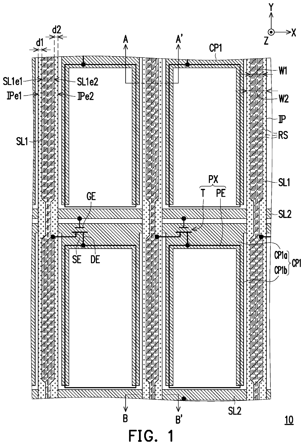
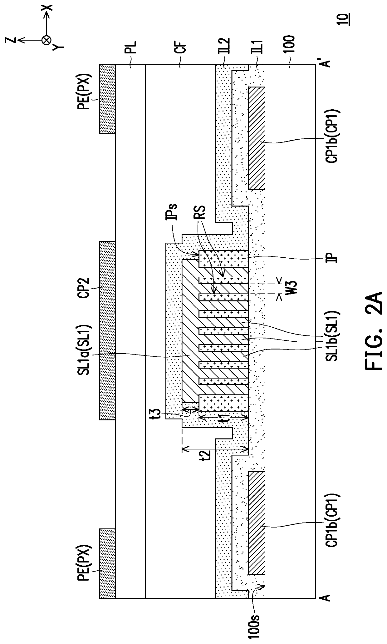
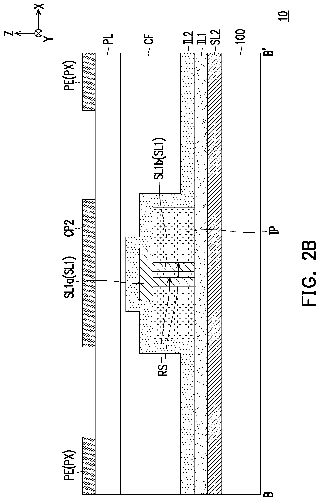
[0019]FIG. 1 is a schematic top view of a pixel array substrate according to the disclosure. FIG. 2A and FIG. 2B are schematic cross-sectional views of the pixel array substrate of FIG. 1. Specifically, for clarity, the illustration of an insulating layer IL1, an insulating layer IL2, a color filter layer CF, a planarization layer PL, and a conductive pattern CP2 of FIG. 2A is omitted in FIG. 1. FIG. 2A and FIG. 2B correspond to the section line A-A′ and the section line B-B′ of FIG. 1, respectively.
[0020]Referring to FIG. 1, FIG. 2A, and FIG. 2B, a pixel array substrate 10 includes a substrate 100, multiple signal lines SL1, multiple signal lines SL2, and multiple pixel structures PX. The signal lines SL1 are disposed along a direction X and extend in the direction Y. The signal lines SL2 are disposed along the direction Y and extend in the direction X. In the embodiment, for example, the signal line SL1 and the signal line SL2 are a data line and a scan line, respectively, but the...
second embodiment
[0039]FIG. 3 is a schematic cross-sectional view of a pixel array substrate according to the disclosure. Referring to FIG. 3, the difference between a pixel array substrate 10A of the embodiment and the pixel array substrate 10 of FIG. 2A is that an insulation pattern IP′ of the pixel array substrate 10A does not have the recess structure RS of FIG. 2A. That is, in the embodiment, the signal line SL1′ does not have the portion SL1b of the signal line SL1 extending into the recess structure RS in FIG. 2A.
[0040]In the embodiment, a thickness t1′ of the insulation pattern IP′ in the thickness direction (e.g., the direction Z) is greater than a thickness t3′ of the signal line SL1′ in the thickness direction. With the configuration of the insulation pattern IP′, the distance between the signal line SL1′ and the conductive pattern CP1 may be increased, thereby suppressing the capacitive coupling effect between the signal line SL1′ and the conductive pattern CP1, which contributes to impr...
third embodiment
[0041]FIG. 4 is a schematic cross-sectional view of a pixel array substrate according to the disclosure. Referring to FIG. 4, the difference between a pixel array substrate 11 of the embodiment and the pixel array substrate 10 of FIG. 2A is that the quantity and the width of the recess structures of the insulation pattern are different. Specifically, the number of recess structures RS-A of an insulation pattern IP-A is two, and a width W3′ of the vertical projection of the recess structure RS-A on the substrate surface 100s in the direction X is significantly greater than the width W3 of the vertical projection of the recess structure RS on the substrate surface 100s of FIG. 2A in the direction X.
[0042]In the embodiment, the width W3′ of the vertical projection of the recess structure RS-A on the substrate surface 100s in the direction X is greater than two times thickness t3″ of the portion of the signal line SL1-A outside the recess structure RS-A in the thickness direction (e.g.,...
PUM
 Abstract
Description
Claims
Application Information


