Foldable OLED display panel
a display panel and foldable technology, applied in static indicating devices, instruments, organic semiconductor devices, etc., can solve problems such as display abnormalities of foldable oled display panels, failure of normal signal transmission, so as to reduce the bending resistance of signal lines, improve the display effect, and reduce the effect of multiple bending
- Summary
- Abstract
- Description
- Claims
- Application Information
AI Technical Summary
Benefits of technology
Problems solved by technology
Method used
Image
Examples
embodiment 1
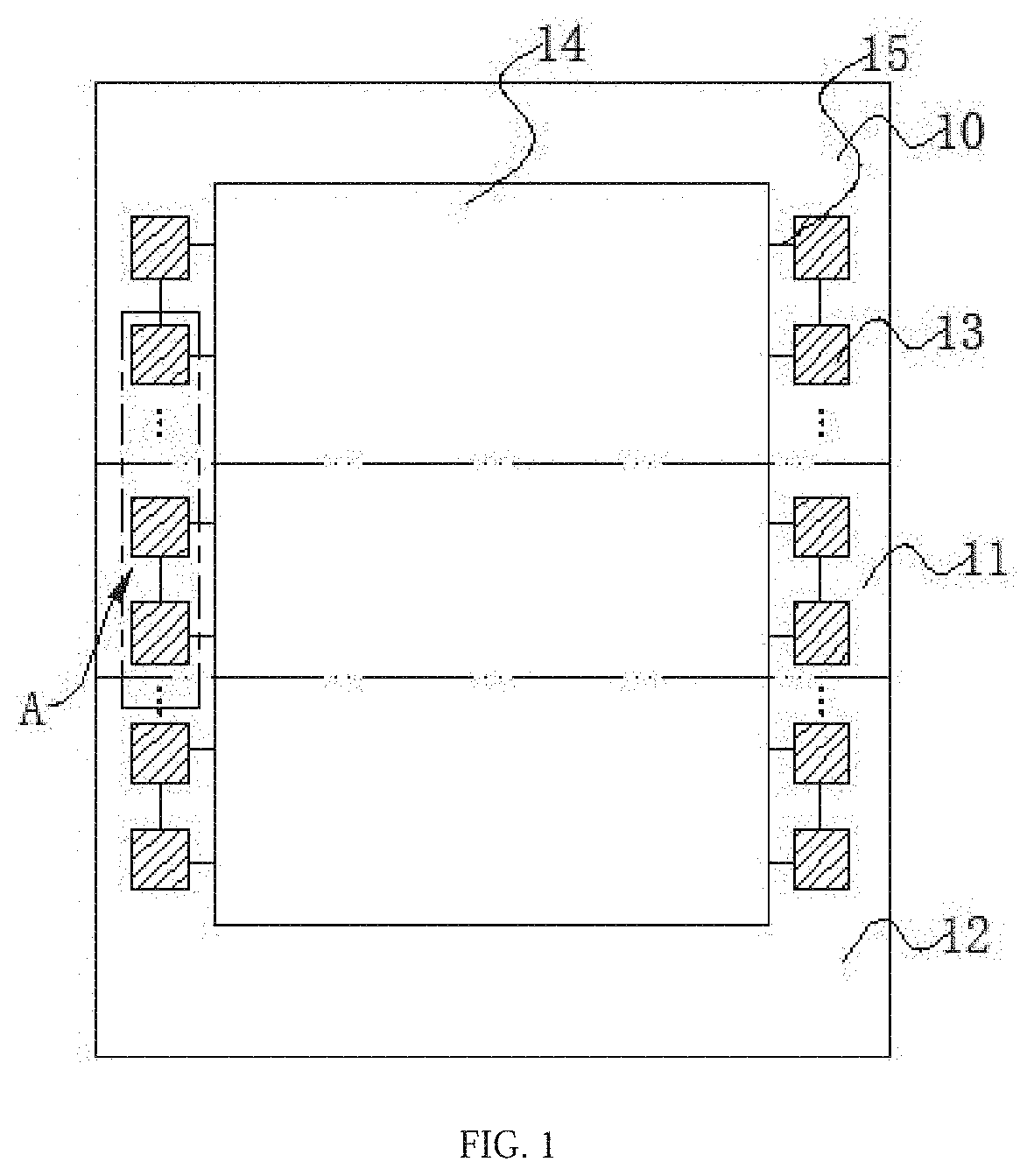
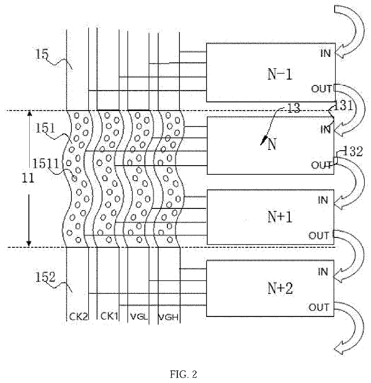
[0034]FIG. 2 is an enlarged schematic view of part A of the foldable OLED display panel according to FIG. 1. The GOA unit circuits 13 of each stage are connected to the signal lines 15 by scanning data lines. The signal lines include GOA signal lines, pixel unit signal lines and power signal lines. The GOA signal lines include first clock signal lines (CK1), second clock signal lines (CK2), voltage gate high (VGH) signal lines and voltage gate low (VGL) signal lines for the GOA unit circuits 13 in regular work.
[0035]Specifically, an input signal (IN) 131 in the GOA unit circuits 13 of a Nth stage is provided by an output signal (OUT) of the GOA unit circuits of a N−1th stage, and a switching signal of the pixel unit of a Nth row and an input signal of the GOA unit circuits of a N+1th stage are provided by an output signal (OUT) 132 of the GOA unit circuits of the Nth stage.
[0036]Specifically, the signal lines 15 further include first sub-signal lines 151 overlapping the folded regio...
embodiment 2
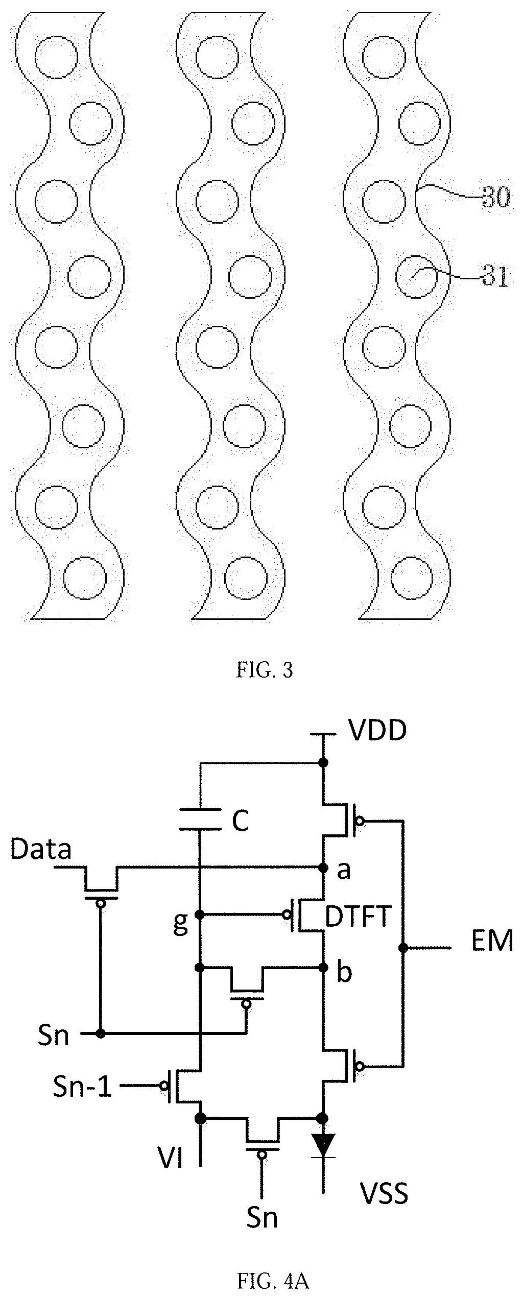
[0039]FIG. 3 is a schematic view of signal lines in a folded region of the foldable OLED display panel according to the present disclosure. The through holes 31 on the surfaces of the signal lines 30 in the folded region are disposed in a single row, and the through holes 31 are arranged along bending paths of the signal lines 30. Preferably, shapes of the through holes 31 are round or oval.
[0040]Refer to FIG. 4A, which is a circuit schematic diagram of a pixel 7T1C of the foldable OLED display panel of the present disclosure. A gate on array (GOA) circuit 7 is composed of seven thin-film transistors (TFT) and one capacitor. Multi-pulses and scanning signals in any shape are generated by a clock signal design.
[0041]Refer to FIG. 4B, which is a circuit layout of the pixel 7T1C of the foldable OLED display panel of the present disclosure. Four first scanning signal lines (GE1) arranged along a horizontal direction correspond to a scanning circuit signal of N−1th stage (Sn−1), a scanni...
PUM
| Property | Measurement | Unit |
|---|---|---|
| shapes | aaaaa | aaaaa |
| flexible | aaaaa | aaaaa |
| impact resistance | aaaaa | aaaaa |
Abstract
Description
Claims
Application Information


