
Image signal processing device

a signal processing and image technology, applied in the field of image signal processing devices, can solve the problems of deteriorating image quality of an image displayed on the screen of the liquid crystal display device, large size of the image signal processing device, etc., and achieve the effect of suppressing the deterioration of image quality

Inactive Publication Date: 2013-02-19
THINE ELECTRONICS
View PDF17 Cites 0 Cited by
  • Summary
  • Abstract
  • Description
  • Claims
  • Application Information

AI Technical Summary

Benefits of technology

[0009]The present invention has been developed in order to solve the above-mentioned problems and an object thereof is to provide an image signal processing device that employs the overdrive technique to acquire corrected image data through encoding processing and decoding processing, which is capable of suppressing the deterioration of image quality due to a flicker etc., and which can be downsized.
[0017]The image signal processing device according to the present invention employs the overdrive technique to acquire corrected image data through encoding processing and decoding processing, is capable of suppressing image quality from deteriorating due to a flicker etc., and can be downsized.

Problems solved by technology

However, the overdrive technique, which acquires the corrected image data G2′ through the encoding processing and the decoding processing as described above, requires two decoding parts, and therefore, the size of the image signal processing device is large.
Further, there may be a case where the influence of the error at the time of the encoding processing and the decoding processing is exerted on the corrected image data G2′ and the error appears large in the corrected image data G2′, and therefore, there may be a case where the image quality of an image displayed on the screen of the liquid crystal display device is deteriorated due to a flicker etc.

Method used


Image

  • Image signal processing device
  • Image signal processing device
  • Image signal processing device

Examples


Embodiment Construction

[0035]Preferred embodiments to embody the present invention are described below in detail with reference to the accompanied drawings. In the description of the drawings, the same symbols are attached to the same components and duplicated description is omitted.

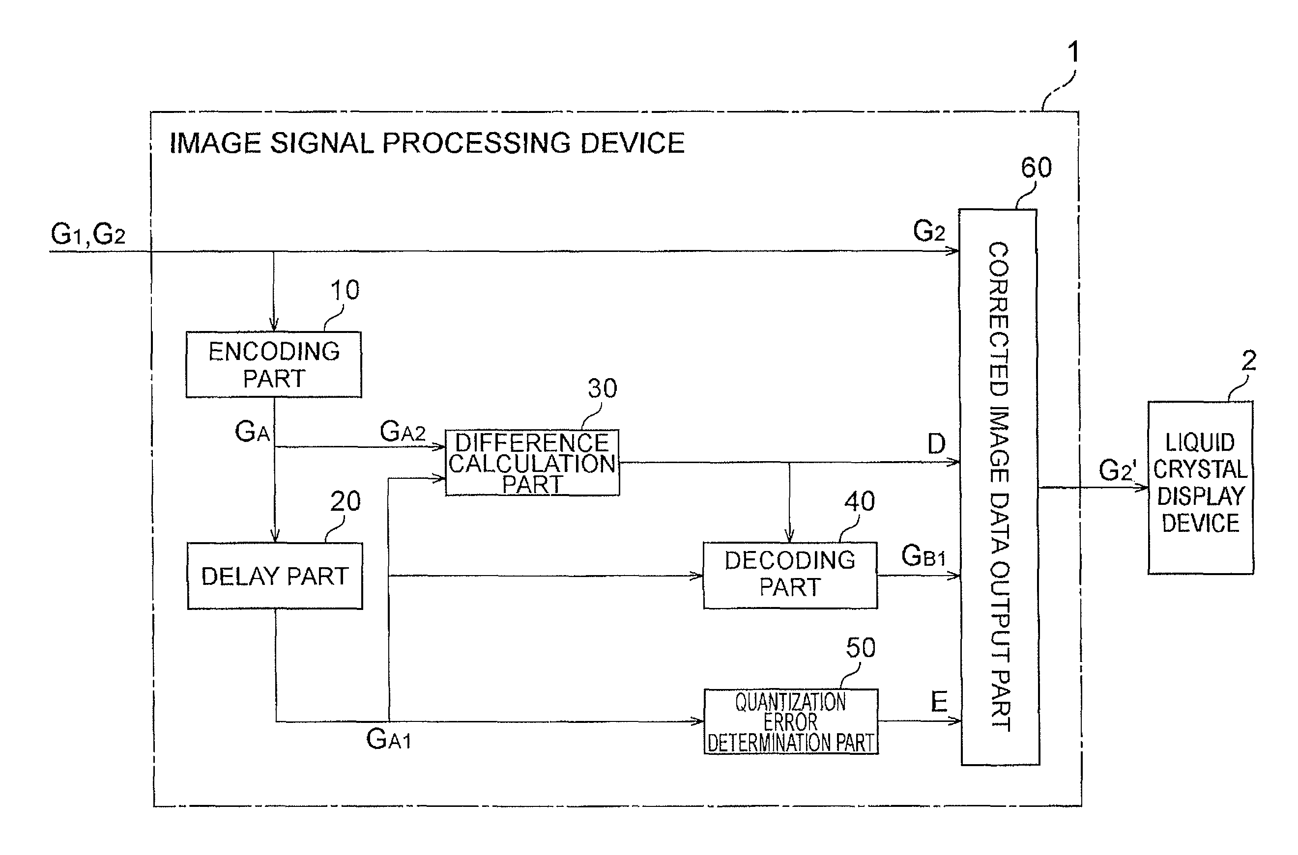
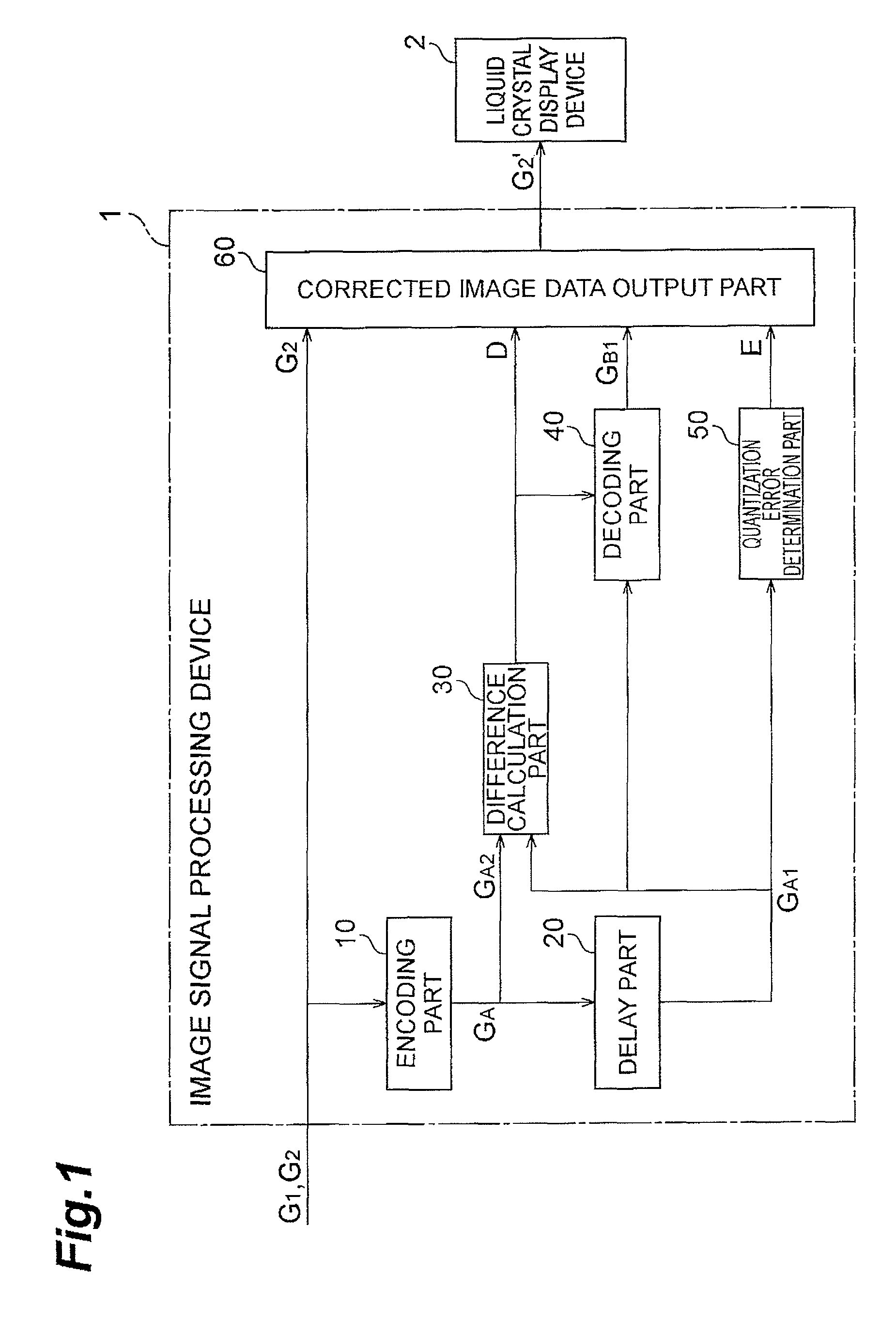
[0036]FIG. 1 is a diagram showing a configuration of an image signal processing device 1 according to the present embodiment. The image signal processing device 1 is configured to output an image signal to a liquid crystal display device 2 after processing image data of each frame of the image signal, comprising an encoding part 10, a delay part 20, a difference calculation part 30, a decoding part 40, a quantization error determination part 50 and a corrected image data output part 60. In the case of a color image, the image data of one color of the color image is described below, however, the description also applies to the image data of the other colors.

[0037]To the encoding part 10, image data of each frame of an image sig...


PUM


Abstract

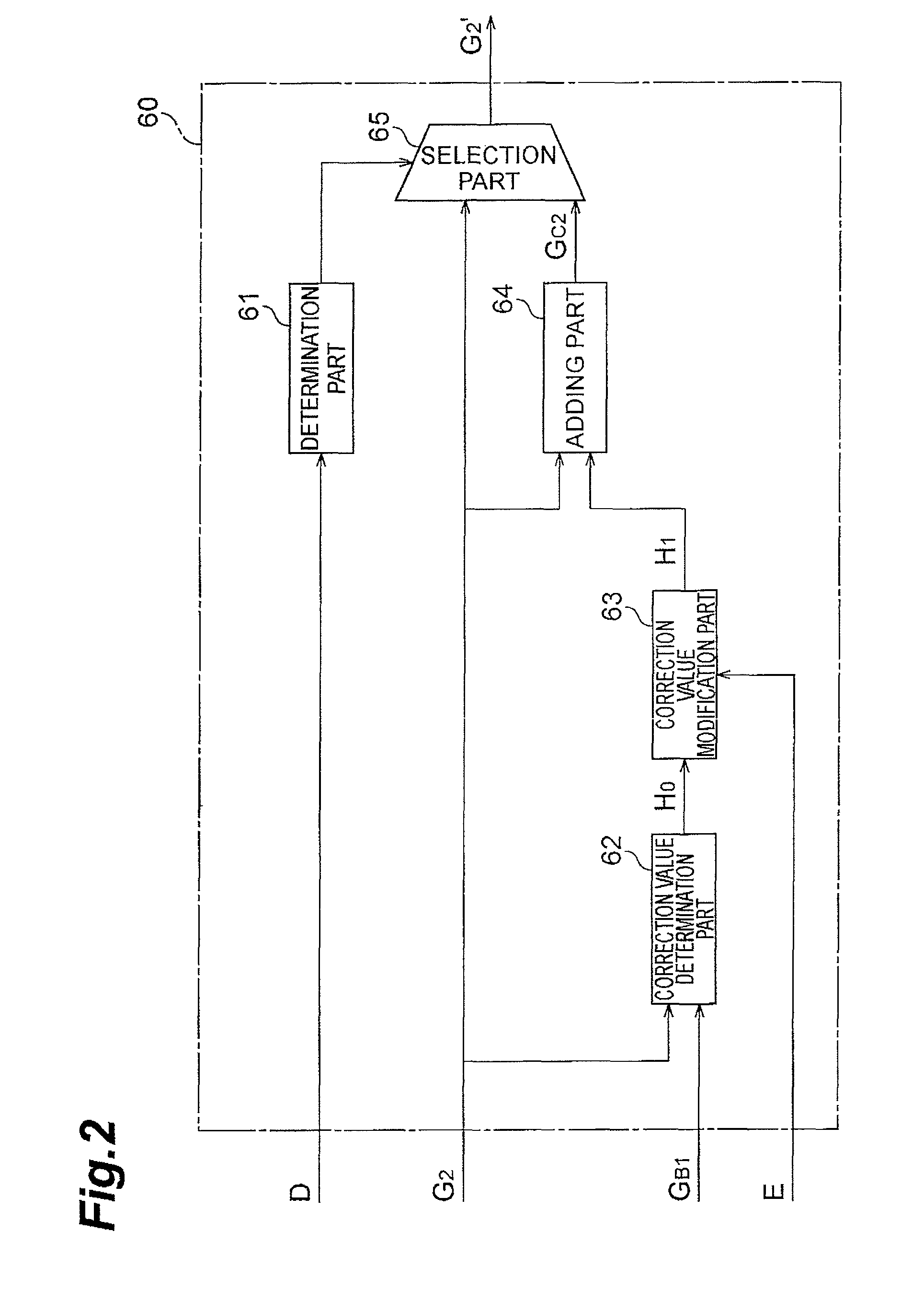
An image signal processing device 1 comprises an encoding part 10, a delay part 20, a difference calculation part 30, a decoding part 40, a quantization error determination part 50 and a corrected image data output part 60. The corrected image data output part 60 outputs image data G2 input to the encoding part 10 as corrected image data G2′ when a difference D output from the difference calculation part 30 is equal to or less than a predetermined value Dth, or determines a basic correction value from the image data G2 input to the encoding part 10 and decoded image data GB1 output from the decoding part 40, reduces the basic correction value by a value in accordance with the magnitude of a quantization error E determined by the quantization error determination part 50 to obtain a modified correction value, and outputs the image data G2 input to the encoding part 10, to which the modified correction value is added, as the corrected image data G2′ when the difference D is greater than the predetermined value Dth.

Description

TECHNICAL FIELD[0001]The present invention relates to an image signal processing device that outputs an image signal to a liquid crystal display device after processing image data of each frame of the image signal.BACKGROUND ART[0002]An image display device is roughly classified into an impulse type display device and a hold type display device. In a CRT (Cathode Ray Tube) mentioned of as an example of an impulse type display device, a screen is scanned by an electron gun and a display is produced only in pixels that electron beams have reached. In contrast to this, in a liquid crystal display device or an organic electroluminescence display device mentioned of as a hold type display device, a frame of an image signal is updated at a fixed period and when a display of an image of a certain first frame is specified, the display of the image of the first frame is held until a display of an image of the next second frame is specified. Compared to an impulse type display device, a hold ...

Claims


Application Information

Patent Timeline
Patent Type & Authority Patents(United States)
IPC IPC(8): G06K9/00H04N7/12H04N5/14G09G3/20G09G3/36H04N5/66H04N19/00H04N19/102H04N19/136H04N19/154H04N19/169H04N19/196H04N19/42H04N19/423H04N19/625H04N19/63H04N19/85H04N19/90
CPCG09G3/3611H04N19/86G09G2320/0247G09G2320/0261G09G2340/16G09G2320/0252
Inventor HIGUCHI, TOMOHISA
Owner THINE ELECTRONICS
Learn More