
Inverter device having separated module terminal

a technology of inverter device and module terminal, which is applied in the direction of substation/switching arrangement details, support structure mounting, printed circuit board receptacles, etc., to achieve the effect of more reliable conditions

Inactive Publication Date: 2013-04-02
KEIHIN CORP
View PDF11 Cites 0 Cited by
  • Summary
  • Abstract
  • Description
  • Claims
  • Application Information

AI Technical Summary

Benefits of technology

[0007]After such studies conducted by the present inventors, the present invention has been completed, and an object of the present invention is to provide an inverter device capable of restraining the affects of the vibrations from the external devices and restraining the positional deviations between the pad surfaces of the insulated substrate and the pad portions of the terminals, with a compact structure.
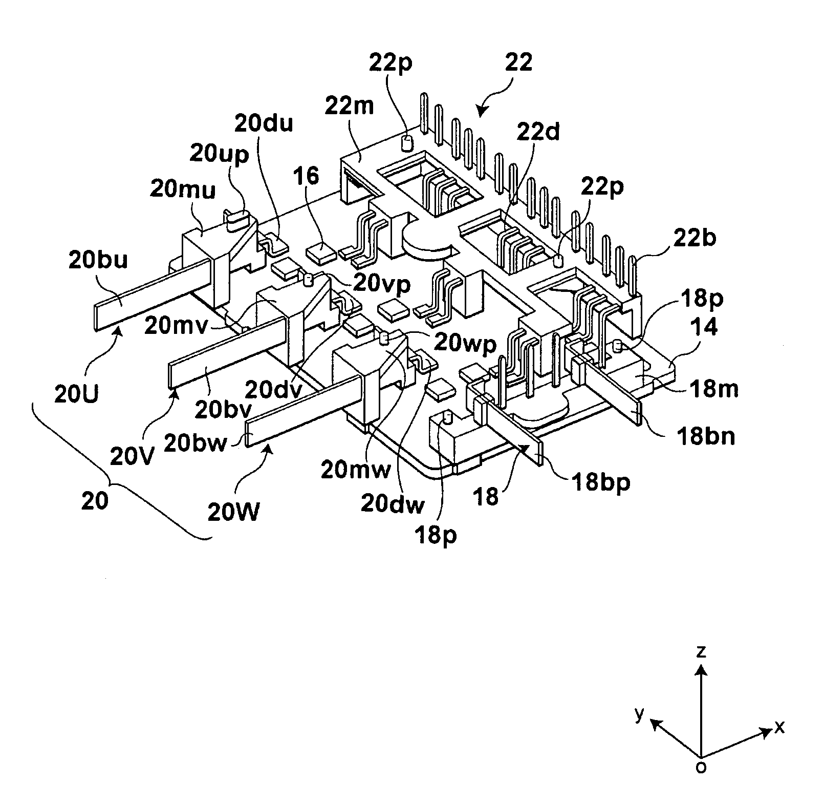
[0009]Due to such an aspect, since the input terminal, the intermediate terminal and the output terminal are made as the separated modules that are spatially independent from each other on the insulated substrate, even in such a situation that a smoothing capacitor is connected with the input terminal (a P terminal and an N terminal), a controller is connected with the intermediate terminal and a load such as a motor and a compressor is connected with the output terminal (a U-phase terminal, a V-phase terminal and a W-phase terminal), mechanical vibrations inputted from the smoothing capacitor and the load can be transmitted to the insulated substrate through the input terminal and the output terminal, correspondingly, and thus mechanical vibrations form such external devices can be prevented form transmitting to the solder connecting portions of the other terminals in direct, thereby realizing the inverter device that is less affected by the mechanical vibrations from surroundings including the external devices. Also, since the input terminal, the output terminal and the intermediate terminal are made as the separated modules that are spatially independent from each other on the insulated substrate, positional deviations between the pad surfaces of the insulated substrate and the pad portions of such terminals can be restrained. Still also, by causing such terminals to form the separated modules that are spatially independent from each other on the insulated substrate, there can be provided the inverter device capable of having a general versatility.
[0011]Due to such an aspect with the depressing member, the connecting state between the insulated substrate and each of the input terminal, the output terminal and the intermediate terminal can be kept in a reliable condition.
[0013]Due to such an aspect with the solder connecting portion and the depressing portion, the connecting state between the insulated substrate and each of the input terminal, the output terminal and the intermediate terminal can be kept in a reliable condition without the stress concentration on the older connecting portion.
[0015]Due to such an aspect with the deformation surface, the connecting state between the insulated substrate and each of the input terminal, the output terminal and the intermediate terminal can be kept in a reliable condition with such a simplified and facilitated structure.
[0017]Due to such an aspect with the split pin, the connecting state between the insulated substrate and each of the input terminal, the output terminal and the intermediate terminal can be kept in a more reliable condition.

Problems solved by technology

Also, since the terminals are unitized as like a single module to the resin-made module case, there are positional deviations between the pad surfaces of the aluminum substrate and the pad portions of the terminals, and it is difficult that the pad portions of the terminals are respectively positioned to the pad surfaces of the aluminum substrate in correct.

Method used


Image

  • Inverter device having separated module terminal
  • Inverter device having separated module terminal
  • Inverter device having separated module terminal

Examples


Embodiment Construction

[0044]Hereinafter, an inverter device having a separated module terminal of an embodiment according to the present invention is described below with suitable reference to the attached drawings. Incidentally, x-axis, y-axis and z-axis form an orthogonal coordinate system.

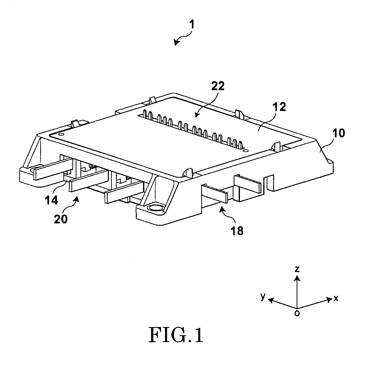
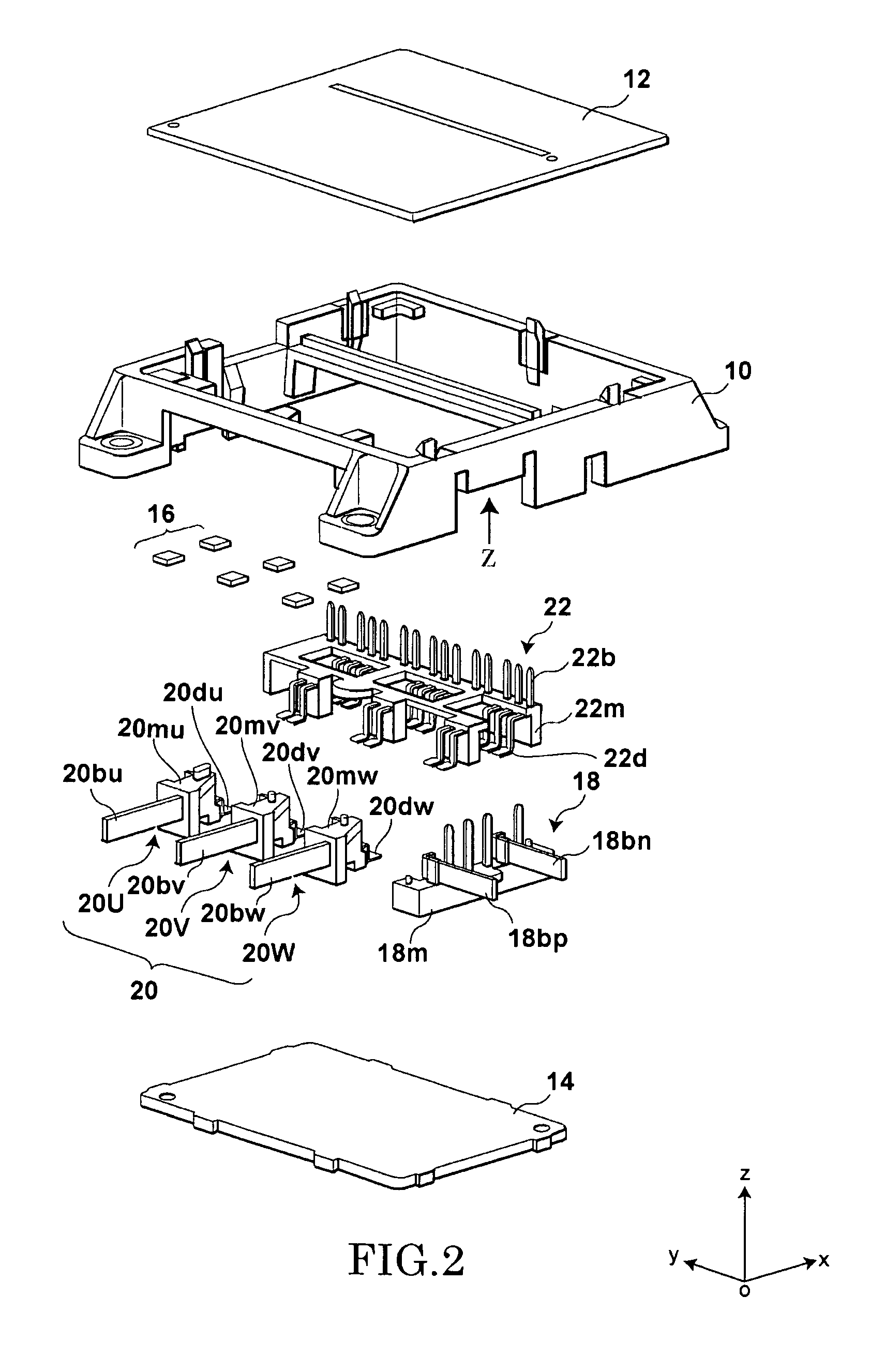
[0045]First, a whole structure of the inverter device having the separated module terminal is described mainly with reference to FIGS. 1 to 4.

[0046]FIG. 1 is a perspective view of the inverter device having the separated module terminal of the present embodiment, and FIG. 2 is an exploded perspective view of the inverter device of the present embodiment. FIG. 3 is a perspective view showing a state in which the separated module terminal and the like are mounted onto an insulated substrate in the inverter device of the present embodiment, and FIG. 4 is a plan view along a negative direction of the z-axis of FIG. 3 of the present embodiment.

[0047]As shown in FIGS. 1 to 4, the inverter device 1 of the present embodiment...


PUM


Abstract

An inverter device is provided with a semiconductor device, an input terminal, an intermediate terminal, an output terminal and an insulated substrate on which the semiconductor device, the input terminal, the intermediate terminal and the output terminal are mounted. Each of the input terminal, the intermediate terminal and the output terminal is a separated module such that one of the input terminal, the intermediate terminal and the output terminal is spatially independent from the other.

Description

BACKGROUND OF THE INVENTION[0001]The present invention relates to an inverter device, and particularly to an inverter device having a separated module terminal on an insulated substrate.[0002]In recent years, a performance required in an electrically driven device such as a motor and a compressor has been highly-developed, and due to such circumstances, an inverter device has been applied to drive the electrically driven device. In such a structure, the inverter device is provided with not only a semiconductor device, such as a transistor, and a controller for controlling an operation of the semiconductor device, but also an input terminal and an output terminal, both for the semiconductor device, and an intermediate terminal connecting the semiconductor device and the controller.[0003]In such a structure, for making the device configuration simple and compact, the input terminal and the like are mounted to a single case as a single piece produced through an integral molding.[0004]S...

Claims


Application Information

Patent Timeline
Patent Type & Authority Patents(United States)
IPC IPC(8): H01R9/00
CPCH05K7/1432H05K7/14322H05K7/14329
Inventor SATO, SHINICHIKISHINO, NORIYAKURIHARA, JIN
Owner KEIHIN CORP
Learn More