Wafer dividing method

a technology of dividing method and dividing chip, which is applied in the direction of manufacturing tools, welding/soldering/cutting articles, metal working apparatuses, etc., can solve the problems of degrading generating debris on the side surface of each device chip obtained, etc., to prevent the degradation of the quality of each device and eliminate the possibility of trouble

Active Publication Date: 2013-04-09
DISCO CORP
View PDF7 Cites 20 Cited by
  • Summary
  • Abstract
  • Description
  • Claims
  • Application Information

AI Technical Summary

Benefits of technology

[0007]It is therefore an object of the present invention to provide a wafer dividing method which can prevent a degradation in quality of each device due to the generation of breaking debris in dividing the wafer and can also eliminate the possibility of trouble in the subsequent steps.
[0009]According to the present invention, the adhesive tape having the adhesive layer capable of being softened by heating is attached to the wafer, and the adhesive tape is next expanded to divide the wafer. Simultaneously with or after this dividing step, the adhesive tape is heated to make the softened adhesive layer enter the space between the adjacent device chips, so that the debris generated on the side surface of each device chip can be caught by the adhesive layer by adhesion. Accordingly, the deposition of the debris to the front side of each device can be prevented to thereby prevent degradation in quality of each device and eliminate the possibility of trouble in the subsequent steps.

Problems solved by technology

However, in the above laser processing method including the steps of applying a laser beam having a transmission wavelength to the wafer to thereby form the modified layers inside the wafer and next applying an external force to the wafer to thereby divide (break) the wafer along the modified layers, there is a problem such that breaking debris are generated on the side surface of each device chip obtained by breaking.
When the breaking debris are deposited to the front side of each device, the quality of each device may be degraded and there is a possibility of trouble in the subsequent steps including bonding and packaging.

Method used


Image

  • Wafer dividing method
  • Wafer dividing method
  • Wafer dividing method

Examples


Embodiment Construction

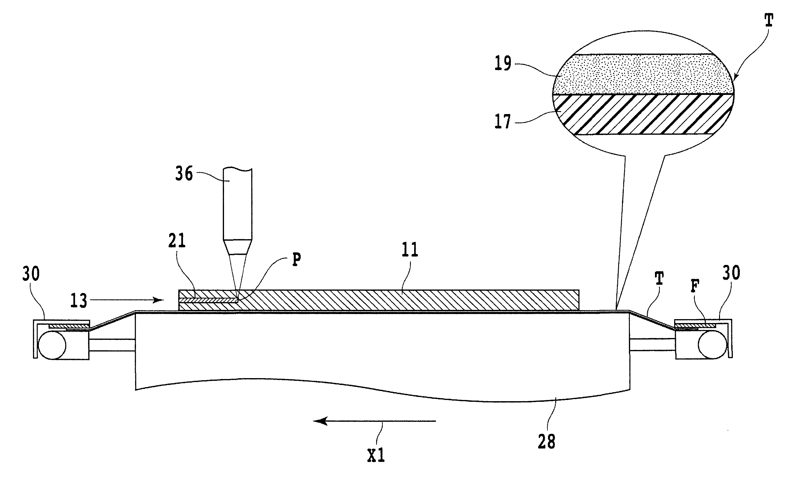
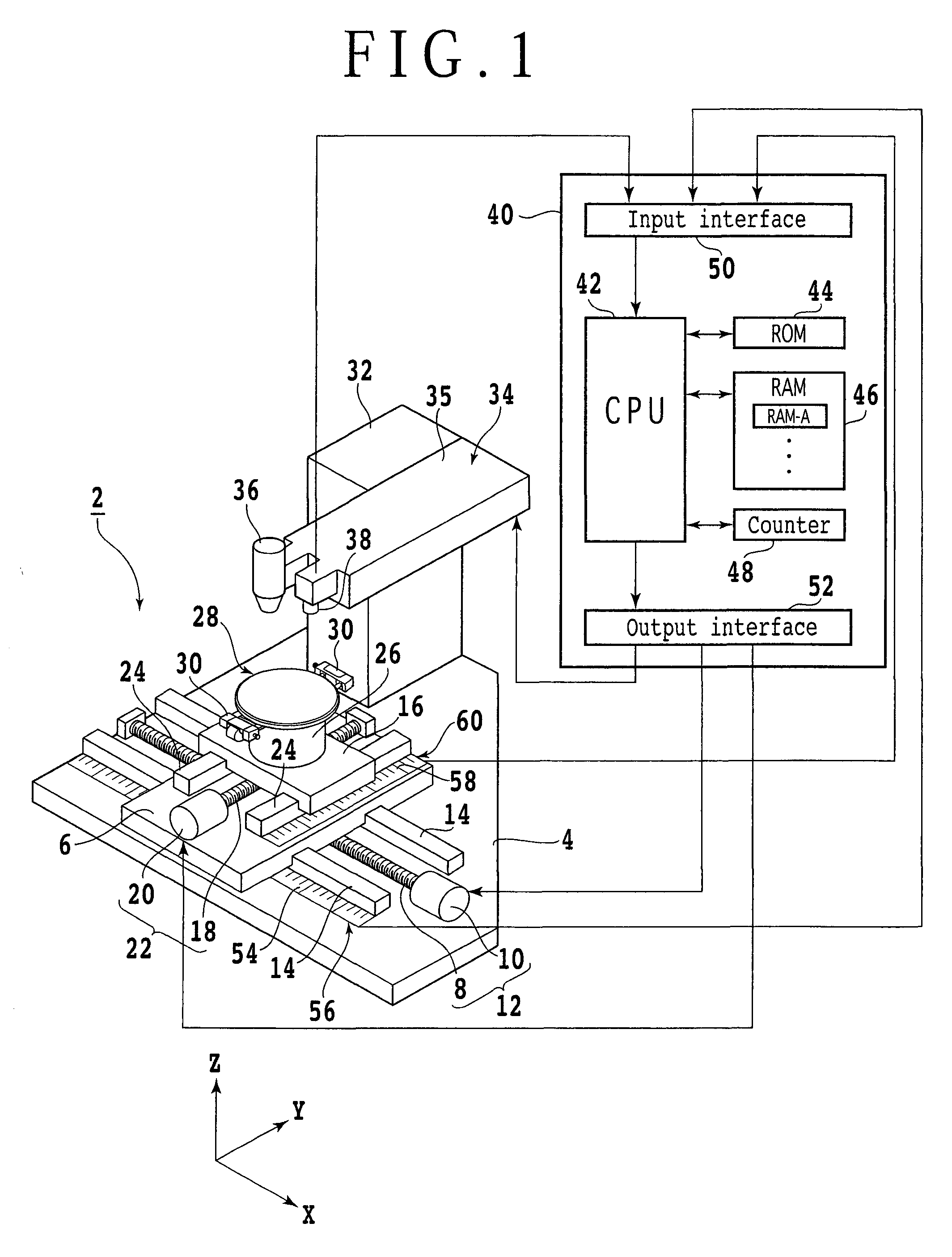
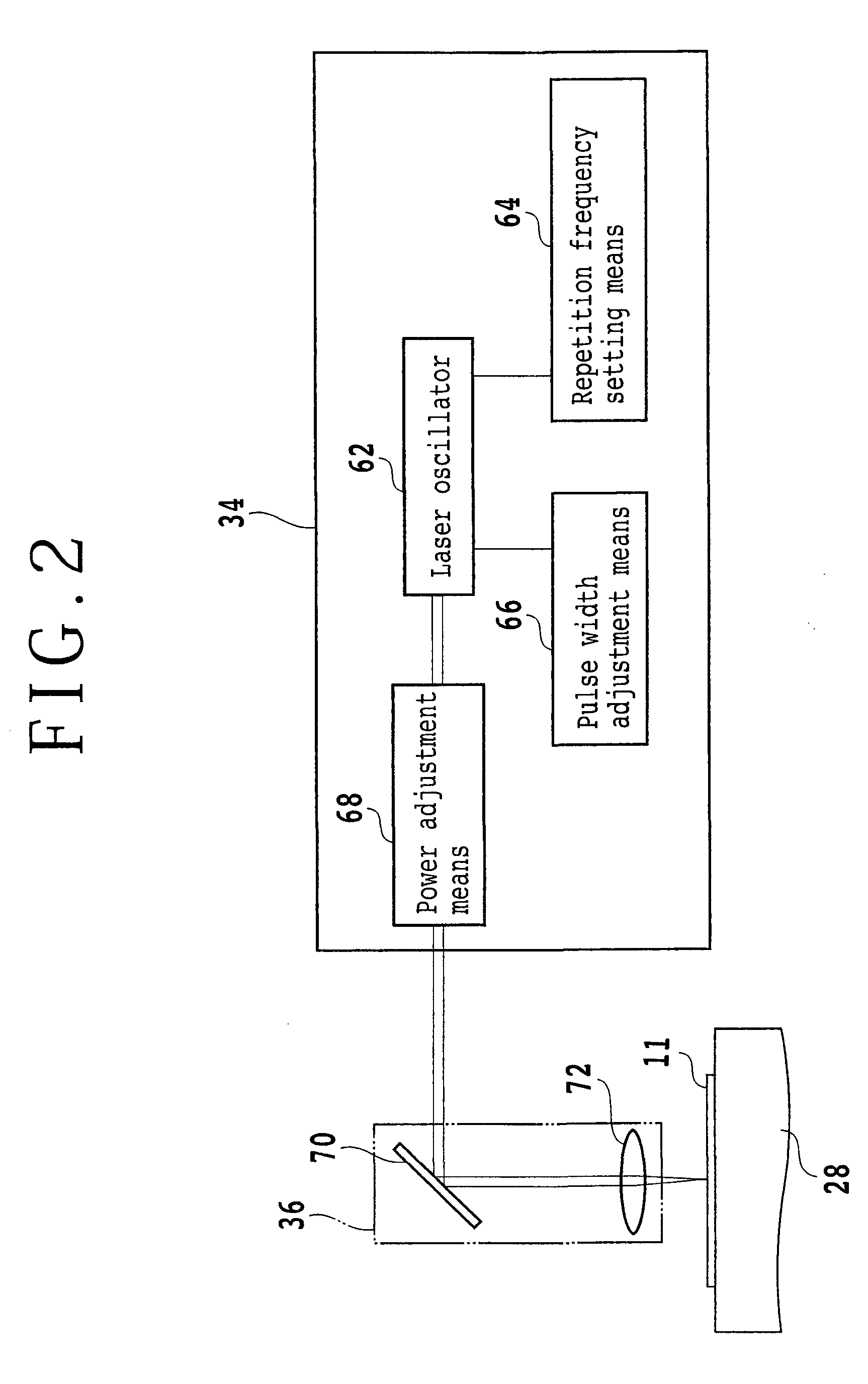
[0019]A preferred embodiment of the present invention will now be described in detail with reference to the drawings. FIG. 1 is a schematic perspective view of a laser processing apparatus 2 for performing the wafer dividing method according to the present invention. The laser processing apparatus 2 includes a stationary base 4 and a first slide block 6 supported to the stationary base 4 so as to be movable in the X direction shown by an arrow X. The first slide block 6 is movable in a feeding direction, i.e., in the X direction along a pair of guide rails 14 by feeding means 12 including a ball screw 8 and a pulse motor 10.

[0020]A second slide block 16 is supported to the first slide block 6 so as to be movable in the Y direction shown by an arrow Y. The second slide block 16 is movable in an indexing direction, i.e., in the Y direction along a pair of guide rails 24 by indexing means 22 including a ball screw 18 and a pulse motor 20. A chuck table 28 is supported through a cylindr...


PUM

PropertyMeasurementUnit
transmission wavelengthaaaaaaaaaa
external forceaaaaaaaaaa
adhesionaaaaaaaaaa

Abstract

A wafer dividing method including a step of applying a laser beam to a wafer along division lines with the focal point of the laser beam set inside the wafer, thereby forming modified layers inside the wafer along the division lines; a step of attaching an adhesive tape to the wafer, the adhesive tape having a base sheet and an adhesive layer; a dividing step of applying an external force to the wafer by expanding the adhesive tape, thereby dividing the wafer along the division lines to obtain a plurality of device chips; and a debris catching step of heating the adhesive tape to thereby soften the adhesive layer such that it enters the space between any adjacent ones of the device chips obtained by the dividing step, thereby catching debris generated on the side surface of each device chip in the dividing step to the adhesive layer by adhesion.

Description

BACKGROUND OF THE INVENTION[0001]1. Field of the Invention[0002]The present invention relates to a wafer dividing method including the steps of applying a laser beam having a transmission wavelength to a wafer to thereby form modified layers inside the wafer and next applying an external force to the wafer to thereby divide the wafer into device chips.[0003]2. Description of the Related Art[0004]In a semiconductor device fabrication process, a plurality of crossing division lines are formed on the front side of a semiconductor wafer to thereby partition a plurality of regions where devices are respectively formed. The semiconductor wafer is cut along the division lines to thereby divide the regions where the devices are formed from each other, thus obtaining individual device chips. Conventionally, cutting of the semiconductor wafer is performed by using a cutting apparatus called a dicing saw. However, it is difficult for the dicing saw to cut an optical device wafer having a cryst...

Claims


Application Information

Patent Timeline
Patent Type & Authority Patents(United States)
IPC IPC(8): H01L21/00H01L21/301
CPCB23K26/0039B23K26/0057B23K26/032B23K26/063B23K26/0853H01L21/6836H01L21/78B23K2201/40H01L2221/68327B23K26/0006B23K26/0622B23K26/53B23K2101/40B23K2103/50
Inventor ABATAKE, JUN
Owner DISCO CORP
Why Eureka
Try Eureka