Data processing circuit with cache and interface for a detachable device

a data processing circuit and detachable device technology, applied in the field of data processing circuits, can solve the problems of reducing system performance, inability to store data, so as to reduce overhead

Active Publication Date: 2013-04-09
NXP BV
View PDF8 Cites 0 Cited by
  • Summary
  • Abstract
  • Description
  • Claims
  • Application Information

AI Technical Summary

Benefits of technology

[0005]Among others, it is an object to provide for a data processing circuit with reduced invalidation of cache data when a device is functionally detached from the circuit and / or reduced need for write back cached data to the detachable device.
[0006]A data processing circuit according to claim 1 is provided. Herein a cache circuit is coupled between a processor and an interface for a detachable device. The cache circuit comprises a cache control circuit configured to write back selectively a part of cached data in response to the flush command. Upon loading a cache line into cache memory the cache control circuit tests whether the cache line has an address within an address range allocated to the detachable device, and if so, it stores an identification covering the cache line for use in flushing. The identification may cover the cache line cache line for example because it contains an address or address part that identifies the cache line, or because the identification represents a range of addresses including the address of the cache line, or because the identification identifies a cache line storage element in which the cache line is stored, for example when each cache line storage element has a flag, by setting a flag for the cache line storage element where the cache line is loaded, or by storing a pointer to the cache line storage element where the cache line is stored. The identification makes it possible to write back selected cache lines quickly, with little circuit overhead during execution of a flush command.
[0009]Common storage space may be used for storing identification of the cache lines for flushing applicable to a plurality of cache circuits. This reduces overhead.

Problems solved by technology

When the detachable device is detached during operation, a problem can arise when data corresponding to the addresses for the detachable device is stored in the cache memory.
After detachment, write back from the cache memory is no longer possible, so that inconsistencies can arise.
One way to circumvent this problem is to avoid all caching data for addresses associated with the detachable device, but this reduces system performance.
However, it has been found that this leads to excessive invalidation of data.

Method used


Image

  • Data processing circuit with cache and interface for a detachable device
  • Data processing circuit with cache and interface for a detachable device
  • Data processing circuit with cache and interface for a detachable device

Examples


Embodiment Construction

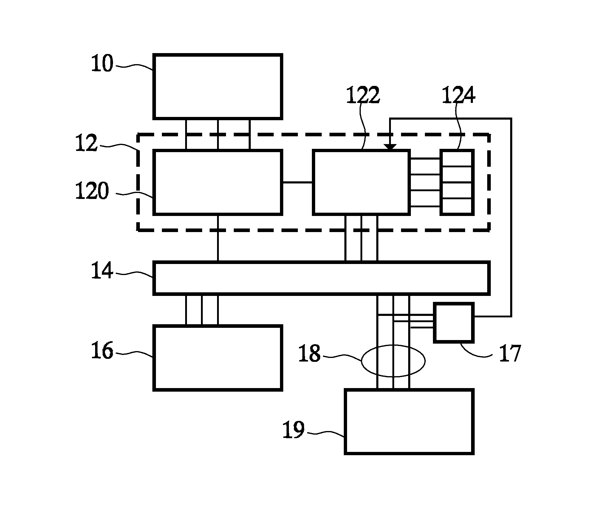
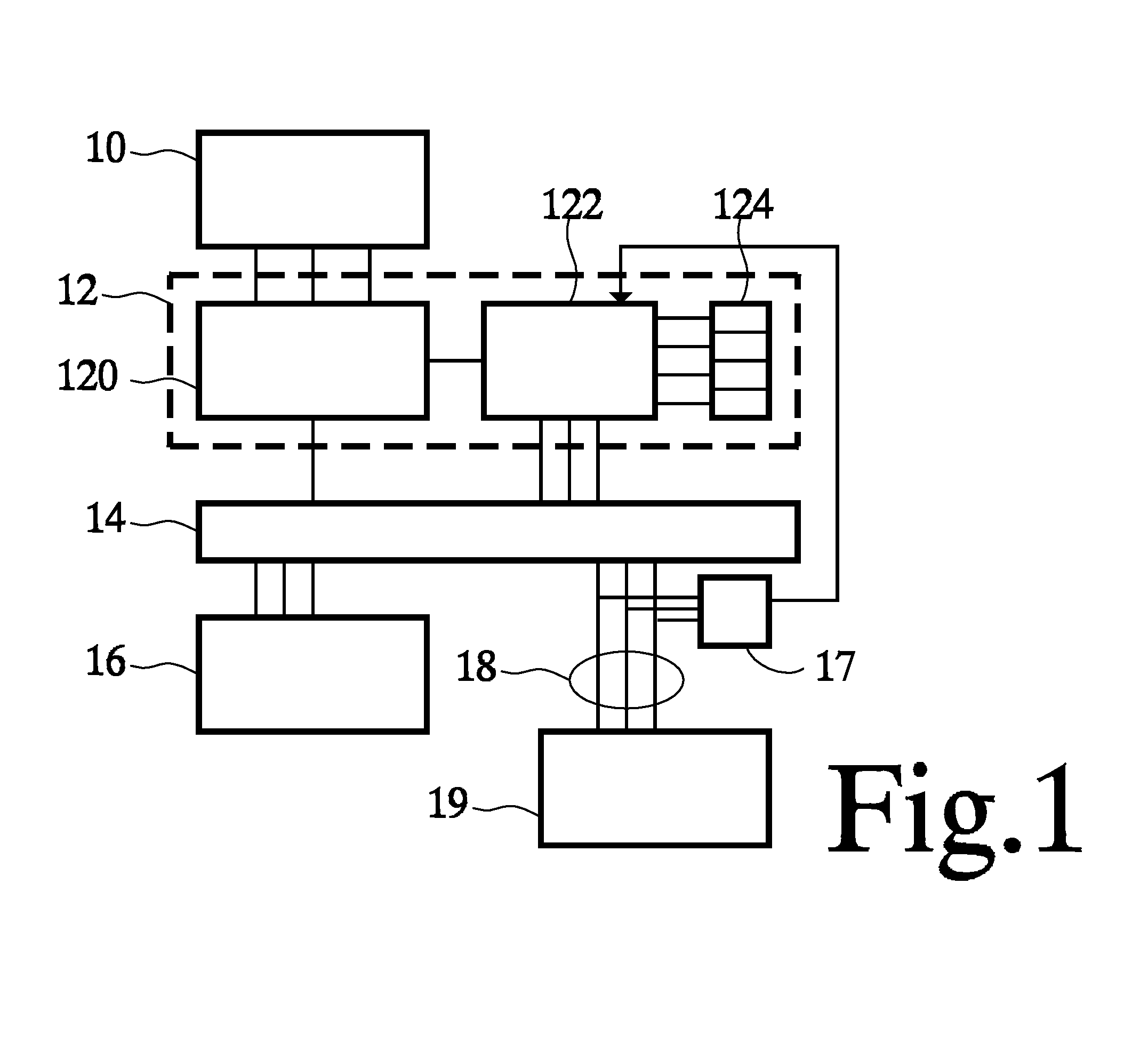
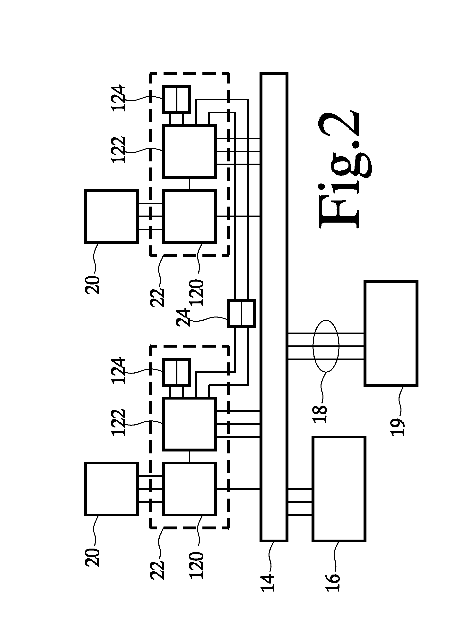
[0013]FIG. 1 shows a data processing circuit, comprising a processor 10, a cache circuit 12, a communication circuit 14, a memory circuit 16, an optional detachment detector 17 and an interface 18 for a detachable device. By way of example a device 19 is shown attached to interface 18. By “detachable” it is meant that device 19 is can be functionally detached in any way during operation, for example by means of physical detachment, or movement out of reception range of a wirelessly communicating device, but also when power supply to the device is cut off or the operating mode of the device is changed so that it is no longer able to receive write back data from the cache memory etc.

[0014]Processor 10 is coupled to communication circuit 14 via cache circuit 12. Via communication circuit 14, the processor 10 and cache circuit 12 are coupled to memory circuit 16 and interface 18. Cache circuit 12 comprises a cache memory 120, a cache control circuit 122 and a set of registers 124. Cache...


PUM


Abstract

A processor (10) of processes data using a cache circuit (12). The processor (20) is coupled to a functionally detachable device (19) via the cache circuit (12). When a cache line is loaded into cache memory (120), it is tested whether the cache line has an address within a detachable device address range allocated to the detachable device (19). If so, identification of the cache line, or a range of addresses that includes the address of the cache line is stored. When a flush command is received that requires write back cached data to the detachable device, the identification is used to select the cache line for selective write back to the detachable device. Thus less cache data needs to be invalidated when a device is functionally detached from the circuit.

Description

FIELD OF THE INVENTION[0001]The invention relates to a data processing circuit and to a method of performing data processing.BACKGROUND OF THE INVENTION[0002]U.S. Pat. No. 5,778,431 discloses a data processing circuit with a dynamically detachable device. A part of the memory space of the data processing circuit is associated with the detachable device. The data processing circuit has a cache memory. When the detachable device is detached during operation, a problem can arise when data corresponding to the addresses for the detachable device is stored in the cache memory. After detachment, write back from the cache memory is no longer possible, so that inconsistencies can arise. Therefore special measures are needed in relation to caching of data from such a detachable device.[0003]One way to circumvent this problem is to avoid all caching data for addresses associated with the detachable device, but this reduces system performance. U.S. Pat. No. 5,778,431 discloses a solution that ...

Claims


Application Information

Patent Timeline
Patent Type & Authority Patents(United States)
IPC IPC(8): G06F12/00G06F13/00G06F13/28G06F12/0804G06F12/0891
CPCG06F12/0804G06F12/0891G06F2212/2146
Inventor LAKSHMI, KRANTHI
Owner NXP BV
Why Eureka
Try Eureka