ESD protection device and method for manufacturing the same
a protection device and electrostatic discharge technology, applied in the direction of shielding materials, semiconductor/solid-state device details, spark plugs, etc., can solve the problems of difficult to achieve the responsivity desired by esd, limited adjustment amount by the size of the product, damage or malfunction of electronic devices, etc., to prevent degradation of discharge characteristics caused by repetitive discharges, and easy to adjust and stabiliz
- Summary
- Abstract
- Description
- Claims
- Application Information
AI Technical Summary
Benefits of technology
Problems solved by technology
Method used
Image
Examples
example 1-1
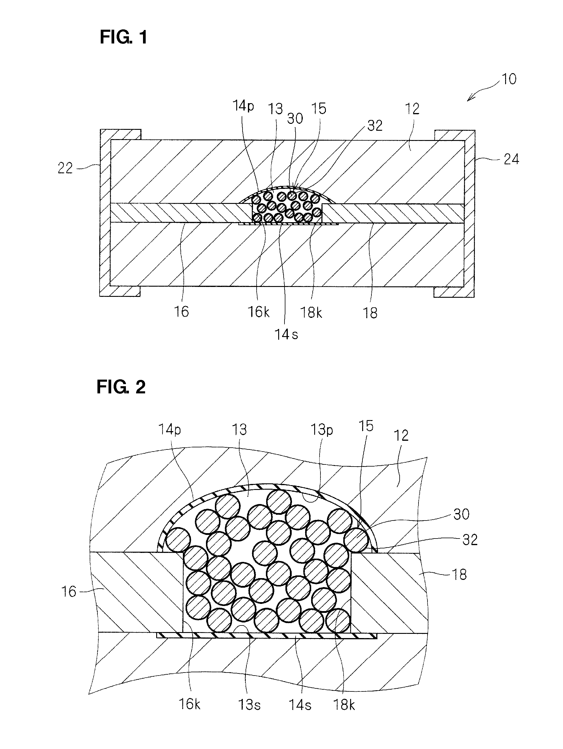
[0122]An ESD protection device 10 of an Example 1-1 of a preferred embodiment of the present invention will be described with reference to FIGS. 1 to 6.
[0123]FIG. 1 is a sectional view of an ESD protection device 10. As shown in FIG. 1, the ESD protection device 10 preferably includes a cavity 13 provided in a substrate body 12 of a ceramic substrate. A pair of discharge electrodes 16 and 18 are arranged such that the respective edges 16k and 18k are exposed in the cavity 13. The discharge electrodes 16 and 18 are arranged so that the edges 16k and 18k face each other with a space provided therebetween. The discharge electrodes 16 and 18 extend to the peripheral surface of the substrate body 12 and are respectively connected to external electrodes 22 and 24 provided on the surface of the substrate body 12. The external electrodes 22 and 24 are used to connect the ESD protection device 10 to another device.
[0124]As schematically shown in FIG. 1, a plurality of supporting electrode pa...
modification 1-1
[0186]A Modification 1-1 of a preferred embodiment of the present invention will be described with reference to FIGS. 7 and 8.
[0187]Modification 1-1 is a modification of Example 1-1. Hereinafter, the same elements and components as those in Example 1-1 are designated by the same reference numerals, and the differences between Example 1-1 and Modification 1-1 will be primarily described.
[0188]FIG. 7 is a sectional view of an ESD protection device 10a of Modification 1-1. FIG. 8 is an enlarged sectional view of a principal portion that shows a cavity 13a of the ESD protection device 10a of Modification 1-1.
[0189]As shown in FIGS. 7 and 8, in the ESD protection device 10a of Modification 1-1, the height of the cavity 13a including a supporting electrode material dispersed therein is substantially equal to the thickness of the discharge electrodes 16 and 18. In other words, a sealing member 14q that defines a top surface 13q of the cavity 13a extends so as to have a planar shape.
[0190]C...
example 1-2
[0191]An ESD protection device of an Example 1-2 of a preferred embodiment of the present invention will be described with reference to FIGS. 9 and 10.
[0192]The ESD protection device of Example 1-2 has substantially the same configuration as that of the ESD protection device 10 of Example 1-1. Hereinafter, the same elements and components as those in Example 1-1 are designated by the same reference numerals, and the differences between Example 1-1 and Example 1-2 will be primarily described.
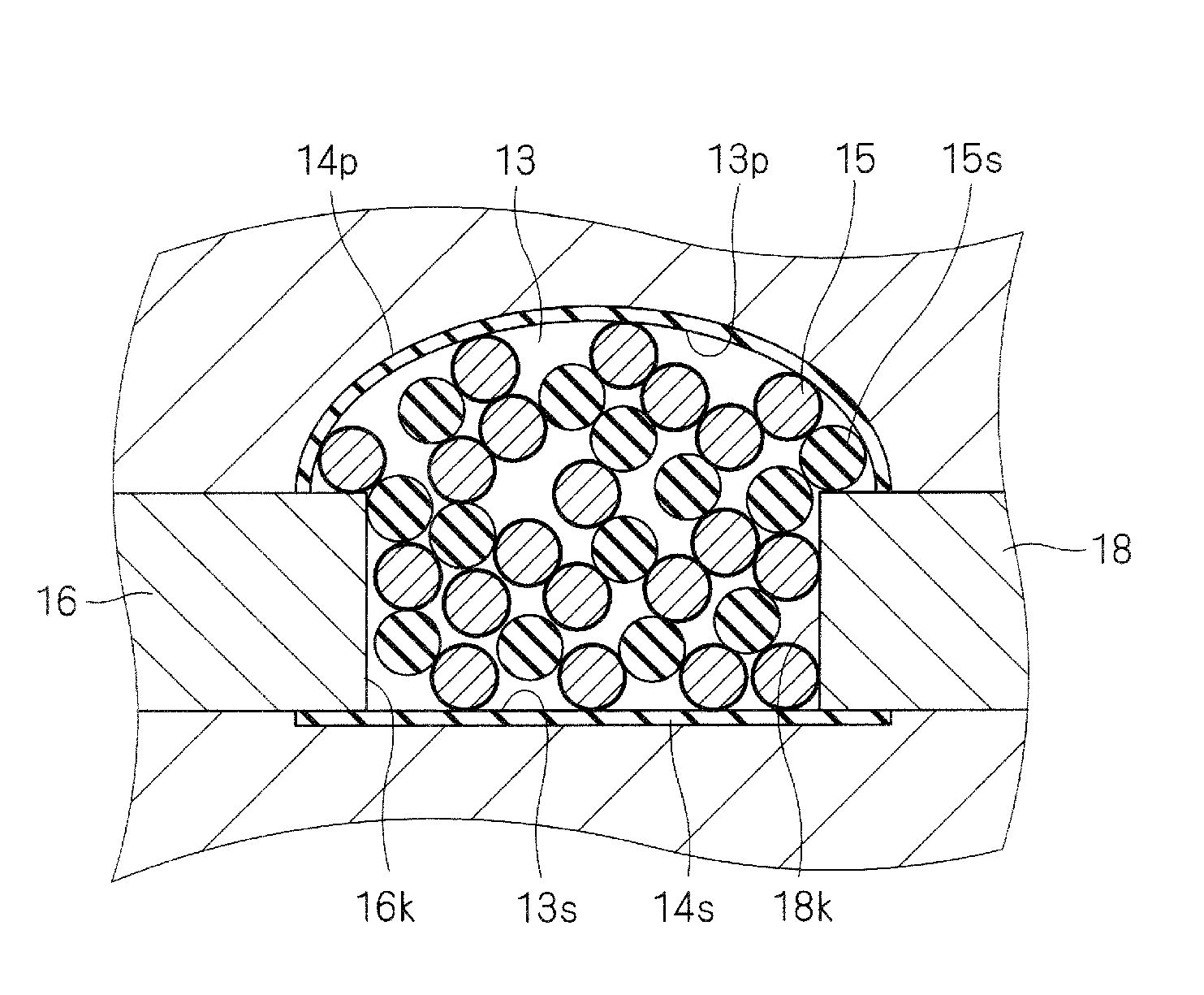
[0193]FIG. 9 is an enlarged sectional view of a principal portion of a cavity 13. As shown in FIG. 9, the ESD protection device of Example 1-2 is different from the ESD protection device 10 of Example 1-1 in that, in addition to the supporting electrode particles 15 including a supporting electrode material, insulating particles 15s are dispersed in the cavity 13. That is, the supporting electrode includes a mixture of the supporting electrode particles 15 and the insulating particles 15s. The pa...
PUM
| Property | Measurement | Unit |
|---|---|---|
| thickness | aaaaa | aaaaa |
| particle size | aaaaa | aaaaa |
| particle size | aaaaa | aaaaa |
Abstract
Description
Claims
Application Information


