ESD protection device

a protection device and electrostatic discharge technology, applied in the direction of emergency protective arrangements for limiting excess voltage/current, emergency protective arrangements, spark gap details, etc., can solve the problems of limited adjustment amount, damage or malfunction of electronic devices, esd protection devices, etc., and achieve easy adjustment and stabilization. , high precision

Active Publication Date: 2011-09-22
MURATA MFG CO LTD
View PDF9 Cites 12 Cited by
  • Summary
  • Abstract
  • Description
  • Claims
  • Application Information

AI Technical Summary

Benefits of technology

[0021]In this case, the ceramic multilayer substrate is preferably a non-shrinkage substrate in which the shrinkage in an in-plane direction of the second ceramic layers is prevented by the first ceramic layers during firing. In the non-shrinkage substrate, almost no warpage and size variation in the in-plane direction are produced. When the non-shrinkage substrate is used for the ceramic multilayer substrate, the space between the discharge electrodes that face each other can be provided with high precision. Consequently, characteristic variations, such as discharge starting voltage, are minimized.
[0022]The ESD characteristics of the ESD protection device of preferred embodiments of the present invention are easily adjusted and stabilized.

Problems solved by technology

ESD causes damage or malfunctioning of electronic devices.
An excessively high voltage, for example, generated by static electricity through an antenna of a mobile phone or other device causes discharge between the discharge electrodes of the ESD protection device, which leads the static electricity to the ground.
However, there are problems with such an ESD protection device.
Furthermore, although the responsivity to ESD can be adjusted by changing an area of the region between discharge electrodes that face each other, the amount of adjustment is limited due to the size of the product.
Therefore, it can be difficult to achieve the desired responsivity to ESD.

Method used


Image

  • ESD protection device
  • ESD protection device
  • ESD protection device

Examples


example 1

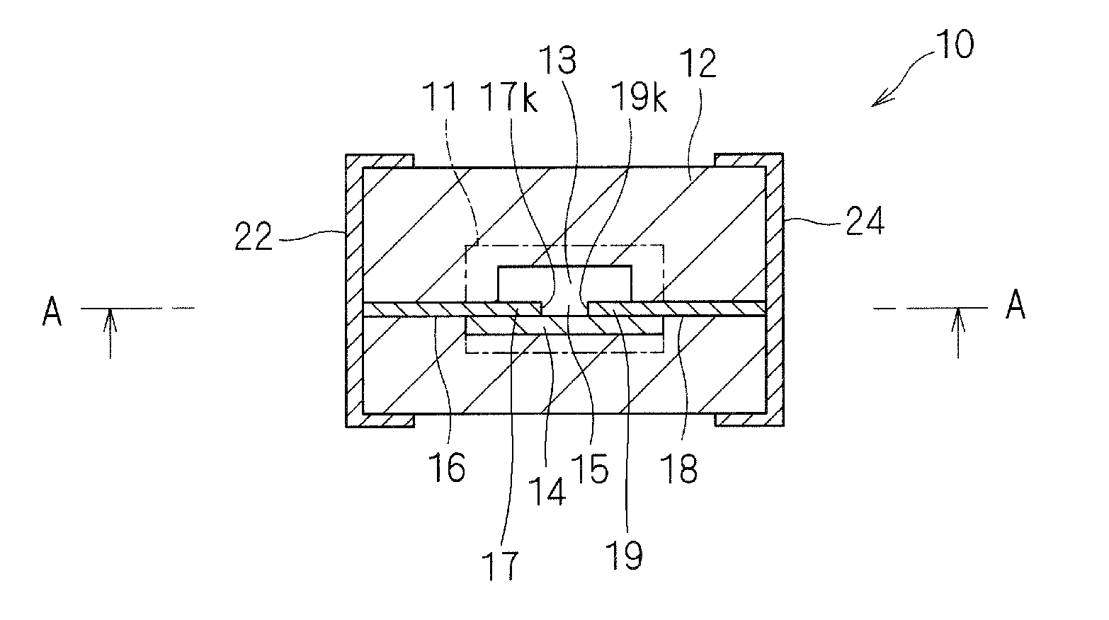
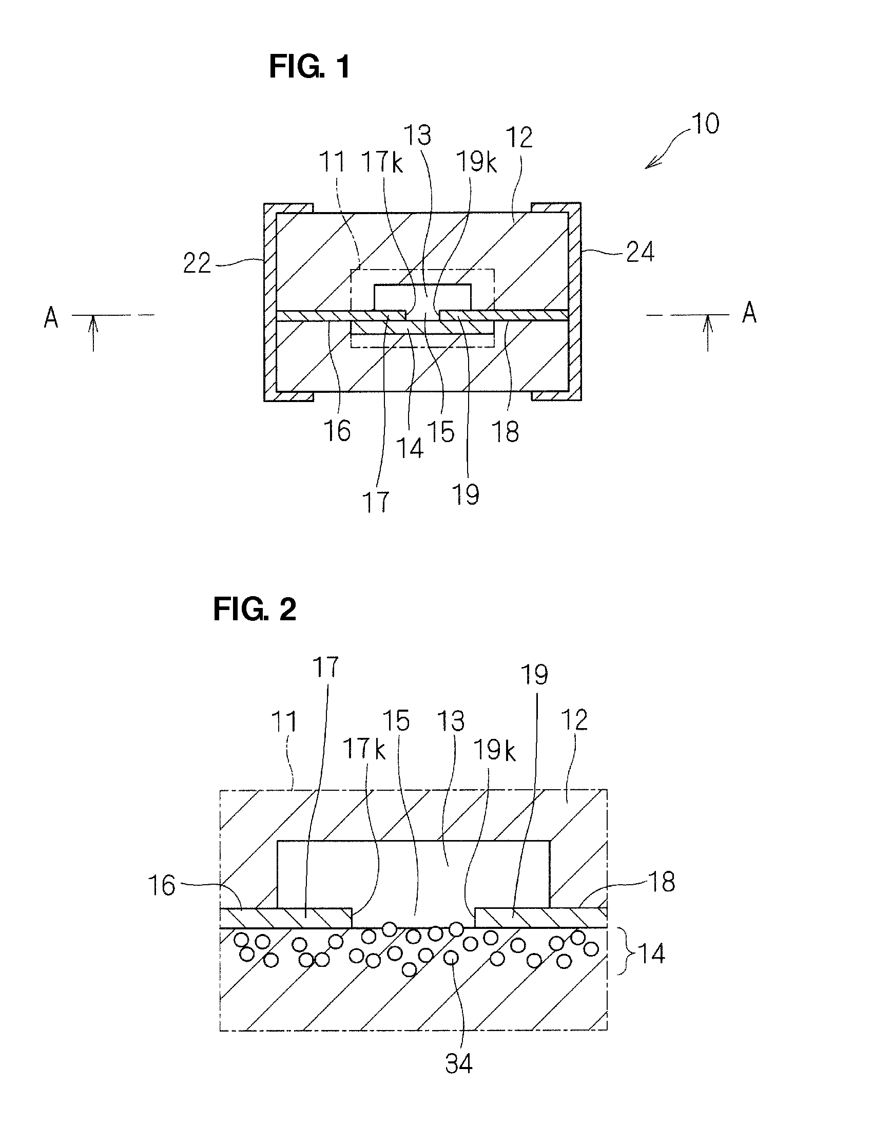
[0031]An ESD protection device 10 of Example 1 will be described with reference to FIGS. 1 to 3. FIG. 1 is a sectional view of the ESD protection device 10. FIG. 2 is an enlarged sectional view of a principal portion schematically showing a region 11 indicated by a chain line of FIG. 1. FIG. 3 is a sectional view taken along line A-A of FIG. 1.

[0032]As shown in FIG. 1, the ESD protection device 10 preferably includes a cavity 13 and a pair of discharge electrodes 16 and 18 provided in a ceramic multilayer substrate 12. The discharge electrodes 16 and 18 preferably respectively include counter portions 17 and 19 arranged along the inner surface of the cavity 13. The discharge electrodes 16 and 18 extend from the cavity 13 to the outer circumferential surface of the ceramic multilayer substrate 12, and are respectively connected to external electrodes 22 and 24 provided on outer surfaces of the ceramic multilayer substrate 12.

[0033]As shown in FIG. 3, edges 17k and 19k of the portions...

example 2

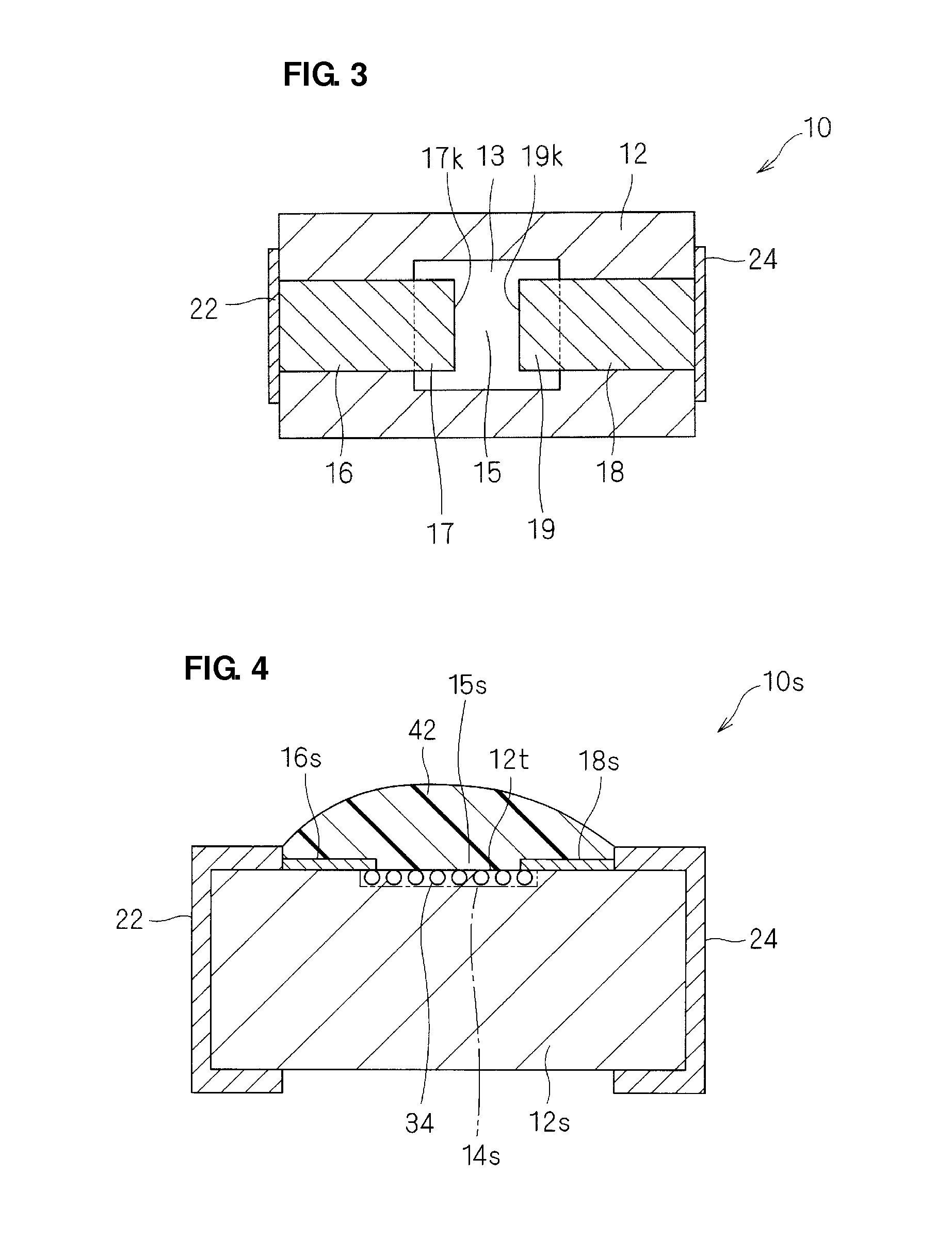
[0066]An ESD protection device 10s of Example 2 according to a preferred embodiment of the preset invention will be described with reference to FIG. 4. FIG. 4 is a sectional view of the ESD protection device 10s.

[0067]The ESD protection device 10s of Example 2 has substantially the same structure as that of the ESD protection device 10 of Example 1. The same components and elements as those in Example 1 are designated by the same reference numerals, and the differences between the ESD protection device 10 of Example 1 and the ESD protection device 10s of Example 2 are primarily described.

[0068]As shown in FIG. 4, the ESD protection device 10s of Example 2 is substantially the same as the ESD protection device of Example 1 except that the ESD protection device 10s preferably does not include the cavity 13. That is to say, the ESD protection device 10s of Example 2 preferably includes a pair of discharge electrodes 16s and 18s that face each other that are provided on an upper surfac...

example 3

[0074]An ESD protection device of Example 3 will be described.

[0075]In a manufacturing example of the ESD protection device of Example 3, the ESD protection device was manufactured by substantially the same method as that of the ESD protection device of Example 1, except that silicon powder was preferably used instead of silicon carbide as the semiconductor material. The particle size of silicon powder was preferably about 1 μm, for example.

[0076]Table 4 shows the conditions of the mixture paste of silicon powder / Cu powder and the evaluation results.

TABLE 4Volume ratio (vol %)DischargeESDSampleSiliconCuShort circuitresponsivitycyclicOverallNo.powderpowdercharacteristicDelaminationto ESDdurabilityevaluation*11000goodpoorgoodgoodpoor29010goodgoodexcellentexcellentexcellent38020goodgoodexcellentexcellentexcellent47030goodgoodexcellentgoodgood56040goodgoodexcellentgoodgood65050goodgoodexcellentgoodgood74060poorpoor——poor83070poorpoor——poor92080poorpoor——poor101090poorpoor——poor*110100po...


PUM

PropertyMeasurementUnit
thicknessaaaaaaaaaa
particle sizeaaaaaaaaaa

Abstract

An ESD protection device includes a ceramic multilayer substrate, at least one pair of discharge electrodes provided in the ceramic multilayer substrate and facing each other with a space formed therebetween, external electrodes provided on a surface of the ceramic multilayer substrate and connected to the discharge electrodes. The ESD protection device includes a supporting electrode obtained by dispersing a metal material and a semiconductor material and being arranged in a region that connects the pair of discharge electrodes to each other.

Description

BACKGROUND OF THE INVENTION[0001]1. Field of the Invention[0002]The present invention relates to an electrostatic discharge (ESD) protection device, and particularly to technologies for preventing breakdown and deformation of a ceramic multilayer substrate caused by, for example, cracking in an ESD protection device that includes discharge electrodes that face each other in a cavity of the ceramic multilayer substrate.[0003]2. Description of the Related Art[0004]ESD is a phenomenon in which strong discharge is generated when a charged conductive body (e.g., human body) comes into contact with or comes sufficiently close to another conductive body (e.g., electronic device). ESD causes damage or malfunctioning of electronic devices. To prevent this, it is necessary to prevent the application of an excessively high voltage generated during discharge to circuits of the electronic devices. ESD protection devices, which are also called surge absorbers, are used for such an application.[00...

Claims


Application Information

Patent Timeline
Patent Type & Authority Applications(United States)
IPC IPC(8): H01L29/86
CPCH01T4/12H01T1/20H01T2/02H01T4/10
Inventor ADACHI, JUNURAKAWA, JUNSUMI, TAKAHIROKITADUME, TAKAHIRO
Owner MURATA MFG CO LTD
Why Eureka
Try Eureka