Shielded embedded electronic component substrate fabrication method and structure

a technology of electronic components and substrates, applied in the direction of semiconductor devices, semiconductor/solid-state device details, electrical devices, etc., can solve the problems of heat transfer from the electronic component, electrical interference between the electronic component and the substrate circuit pattern,

Active Publication Date: 2013-04-30
AMKOR TECH SINGAPORE HLDG PTE LTD
View PDF23 Cites 63 Cited by
  • Summary
  • Abstract
  • Description
  • Claims
  • Application Information

AI Technical Summary

Benefits of technology

[0007]A shielded embedded electronic component substrate includes a core dielectric layer having a die opening. An electrically conductive die shield lines the die opening. An electronic component is mounted within the die opening and to the die shield, where the die shield shields the electronic component. By mounting the electronic component within the die opening, the shie

Problems solved by technology

Unfortunately, mounting the electronic component inside of the substrate causes electromagnetic interference between the electronic component and the substrate circuit patterns due to the close proximity of the electronic

Method used


Image

  • Shielded embedded electronic component substrate fabrication method and structure
  • Shielded embedded electronic component substrate fabrication method and structure
  • Shielded embedded electronic component substrate fabrication method and structure

Examples


Embodiment Construction

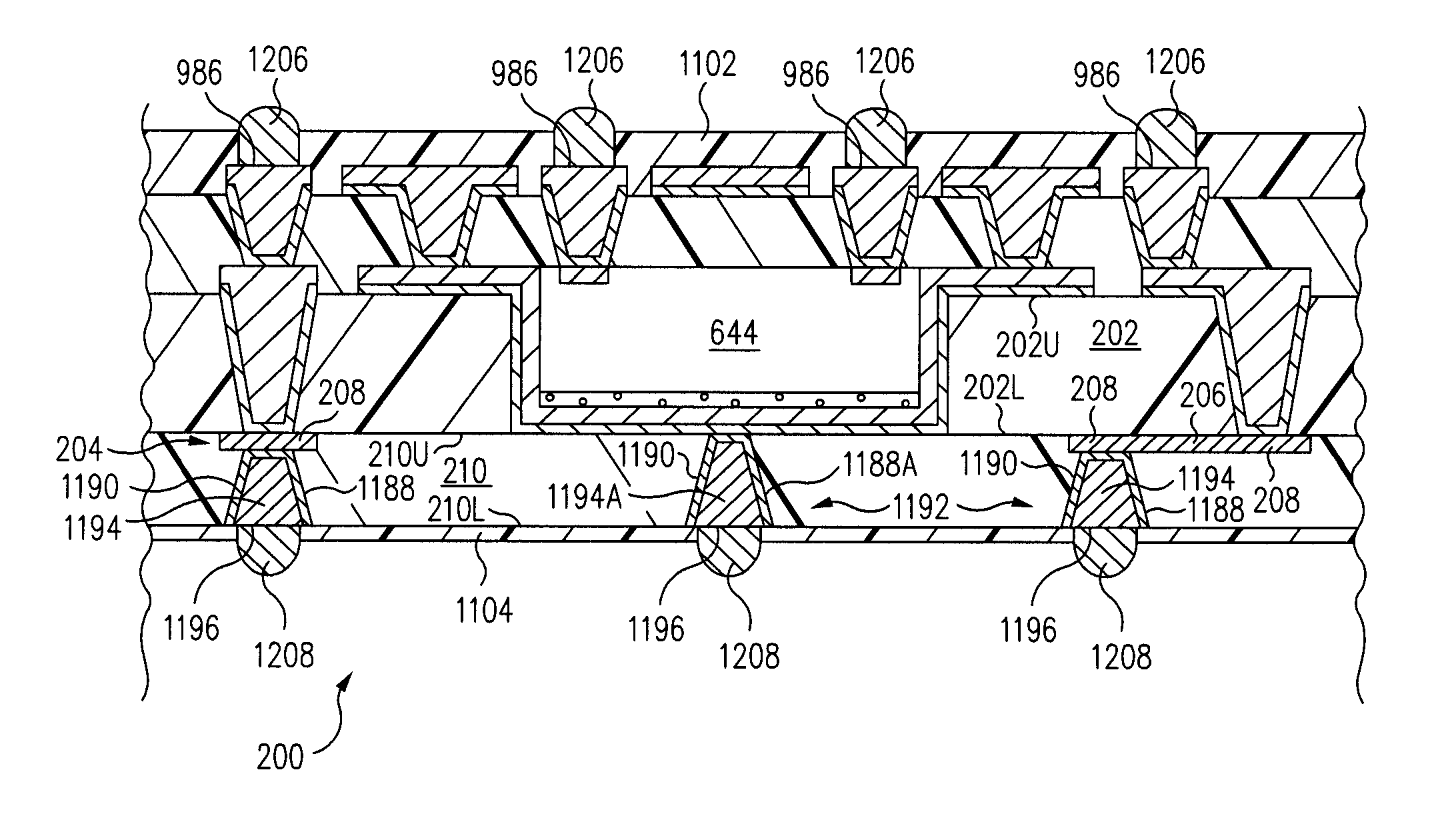
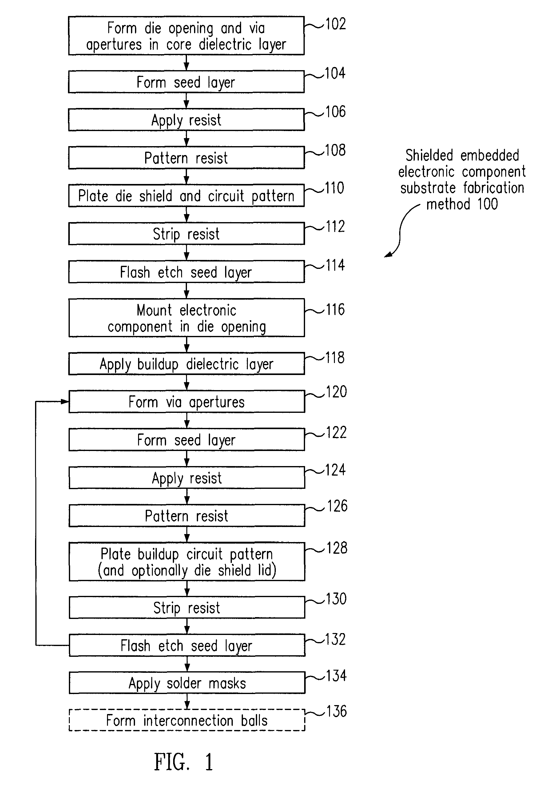
[0018]FIG. 1 is a shielded embedded electronic component substrate fabrication method 100 in accordance with one embodiment. FIG. 2 is a cross-sectional view of a shielded embedded electronic component substrate 200 during fabrication in accordance with one embodiment.

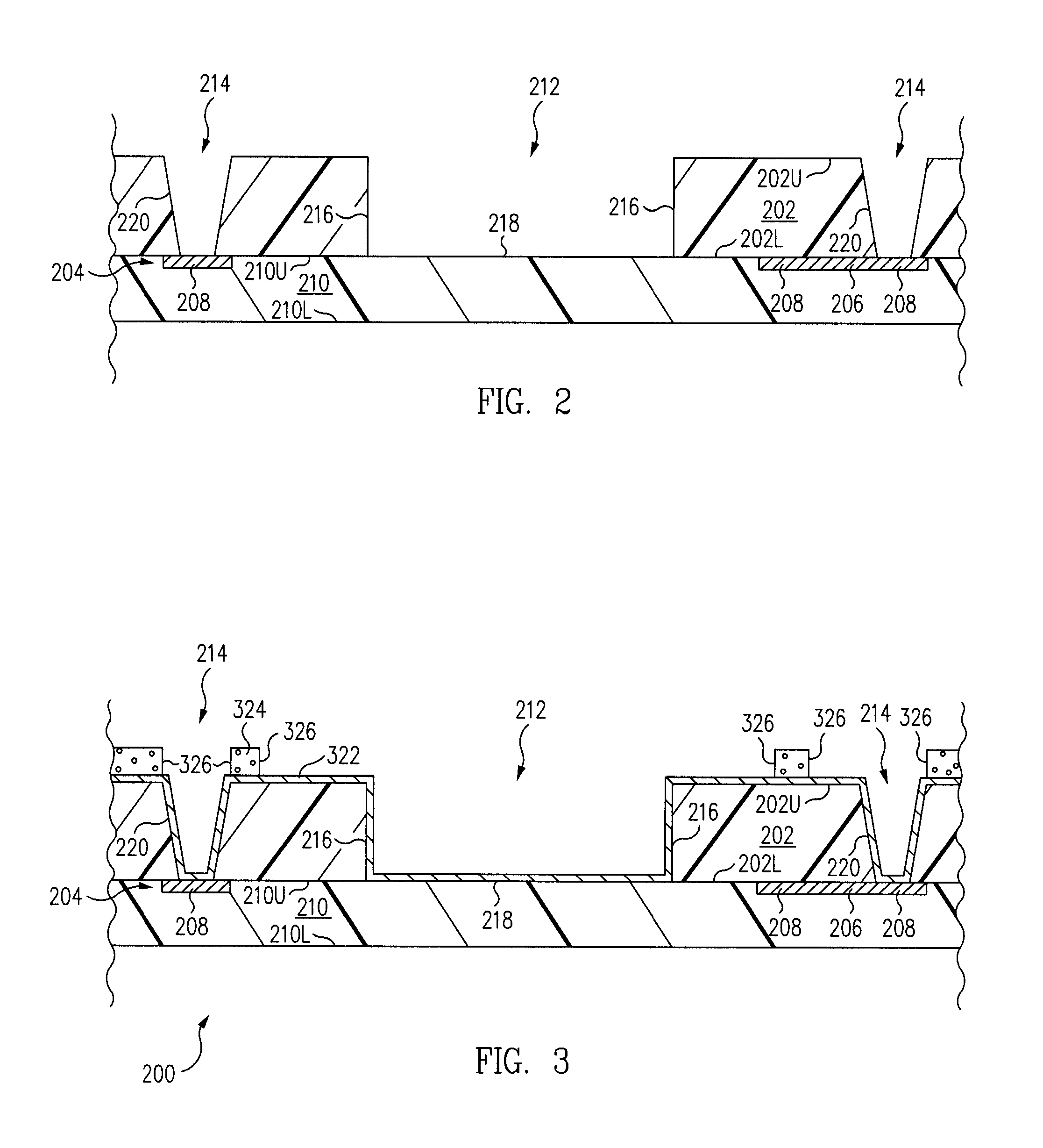
[0019]Referring now to FIGS. 1 and 2 together, shielded embedded electronic component substrate 200 includes a core dielectric layer 202, e.g., prepreg, film and / or laminate. Core dielectric layer 202 includes an upper, e.g., first, surface 202U and a lower, e.g., second, surface 202L.

[0020]Formed on lower surface 202L of core dielectric layer 202 is a lower, e.g., first, circuit pattern 204. Lower circuit pattern 204 is formed of an electrically conductive material such as copper. Lower circuit pattern 204 includes electrically conductive traces 206 and electrically conductive lands 208 in this embodiment.

[0021]Shielded embedded electronic component substrate 200 further includes a lower, e.g., first, buildup dielectr...


PUM


Abstract

A shielded embedded electronic component substrate includes a core dielectric layer having a die opening. An electrically conductive die shield lines the die opening. An electronic component is mounted within the die opening and to the die shield, where the die shield shields the electronic component. By mounting the electronic component within the die opening, the shielded embedded electronic component substrate is made relatively thin. Further, heat generated by the electronic component is dissipated to the die shield and to the ambient environment. Accordingly, the shielded embedded electronic component substrate is well suited for use when the electronic component generates a significant amount of heat, e.g., in high power applications.

Description

BACKGROUND OF THE INVENTION[0001]1. Field of the Invention[0002]The present invention relates generally to methods of fabricating electronic component substrates and the resulting structures. More particularly, the present invention relates to methods of fabricating a shielded embedded electronic component substrate and the resulting structures.[0003]2. Description of the Related Art[0004]To reduce overall package thickness, an electronic component is placed inside of an opening in a substrate. By placing the electronic component inside of the opening in the substrate, the resulting electronic component package is thin relative to an electronic component package having the electronic component mounted on top of the substrate.[0005]Unfortunately, mounting the electronic component inside of the substrate causes electromagnetic interference between the electronic component and the substrate circuit patterns due to the close proximity of the electronic component to the substrate circuit...

Claims


Application Information

Patent Timeline
IPC IPC(8): H01L23/552H01L21/70
CPCH01L23/552H01L24/19H01L21/70H01L2224/0401H01L2224/04105H01L2924/15331H01L2224/32245H01L2224/73267H01L2924/15153H01L2924/15311H01L2224/12105H01L2224/92144H01L2224/2518
Inventor HUEMOELLER, RONALD PATRICKDUNLAP, BRETTHINER, DAVID JON
Owner AMKOR TECH SINGAPORE HLDG PTE LTD
Why Eureka
Try Eureka