Information processing system and control method thereof

a technology of information processing system and control method, which is applied in the field of information processing system, can solve the problems of degrading the operation performance of the master lsi b>10/b>, and achieve the effect of increasing the throughput capacity of the information processing system

Inactive Publication Date: 2013-04-30
RENESAS ELECTRONICS CORP
View PDF13 Cites 1 Cited by
  • Summary
  • Abstract
  • Description
  • Claims
  • Application Information

AI Technical Summary

Benefits of technology

[0032]As shown in FIG. 8, the slave LSI 20 and the ROM 30 are connected in parallel to the master LSI 10 through the SRAM interface bus 40. Therefore, as described in the read operation of FIG. 9, latency including the internal access time Tacs from when the master LSI 10 accesses the slave LSI 20 to when the read data is output to the SRAM interface bus 40 occurs. During the latency period, the SRAM interface bus 40 is occupied only for the access of the master LSI 10 and the slave LSI 20. Therefore, during the latency period, the master LSI 10 cannot access the ROM 30 and read the stored data, which raises an issue that the operating performance of the master LSI 10 is degraded. It is thus desirable to implement a mechanism for minimizing the latency from when the master LSI 10 accesses the slave LSI 20 to when the read data is output to the SRAM interface bus 40.
[0035]According to the exemplary aspects of the present invention, the slave controller can perform determination of the data read operation regardless of the output enable signal that is activated after a predetermined period from the latch timing of the address signal, and, when activated, causes determination of the data read operation on the internal memory space. It is thereby possible to make determination of the data read operation before the output enable signal is activated, thus allowing the data read operation to be started early. This enables reduction of the period during which the interface bus is occupied for the access of the master controller and the slave controller. In this manner, it is possible to reduce the period during which the interface bus is occupied by the master controller and the slave controller and thereby ensure the accessible time of the master controller and the storage circuit, which leads to an increase in the throughput capacity of the information processing system.
[0036]In the information processing system according to the above exemplary aspects of the present invention, it is possible to increase the throughput capacity.

Problems solved by technology

However, because the write data is not output from the master LSI 10 at this point of time, the write operation is not performed, and it enters a write data waiting mode.
Therefore, during the latency period, the master LSI 10 cannot access the ROM 30 and read the stored data, which raises an issue that the operating performance of the master LSI 10 is degraded.

Method used


Image

  • Information processing system and control method thereof
  • Information processing system and control method thereof
  • Information processing system and control method thereof

Examples


first exemplary embodiment

[First Exemplary Embodiment]

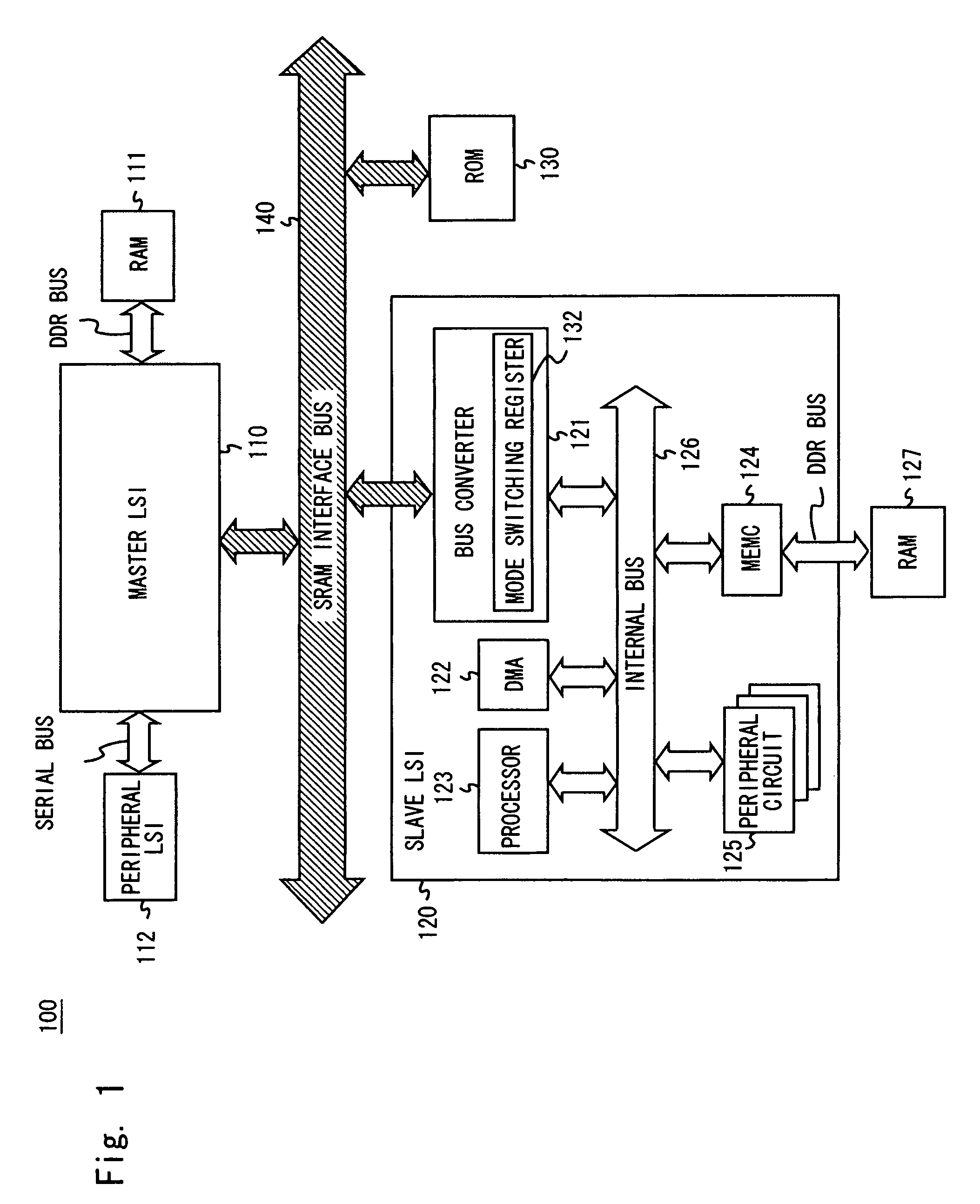
[0048]A first exemplary embodiment of the present invention is described hereinafter in detail with reference to the drawings. FIG. 1 shows an example of a block configuration of an information processing system 100 according to the first exemplary embodiment. The information processing system 100 includes a master LSI 110, a slave LSI 120, ROM 130, and an SRAM interface bus 140. In this manner, the information processing system 100 constitutes a system in which a plurality of LSIs (the ROM 130 is also regarded as one LSI) are integrated, and the plurality of LSIs are connected through the SRAM interface bus 140.

[0049]The master LSI 110, the slave LSI 120 and the ROM 130 are connected to the SRAM interface bus 140. The SRAM interface bus 140 is an AD-mux SRAM interface bus in which an address signal and a data signal are transmitted through a common bus line. Various control signals, the address signal and the data signal in conformity with the AD-mux SRA...

second exemplary embodiment

[Second Exemplary Embodiment]

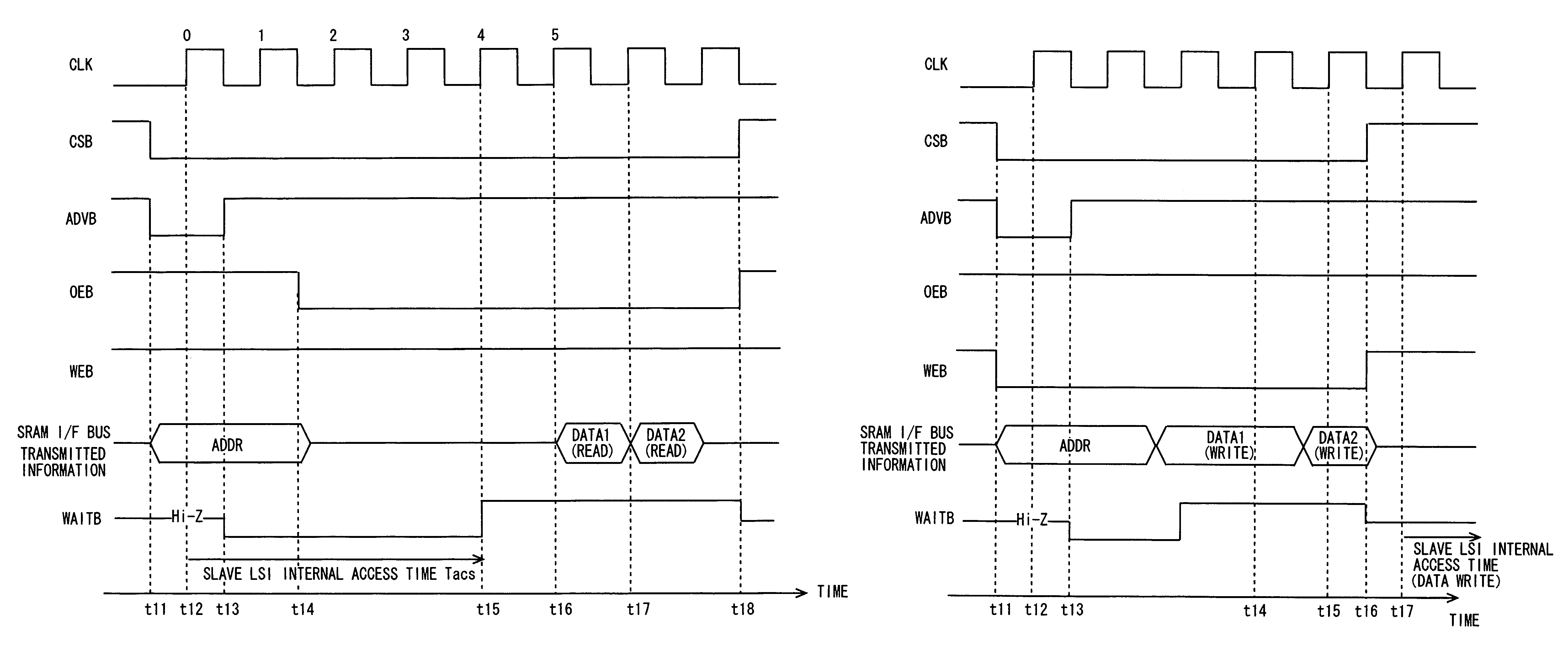
[0091]A second exemplary embodiment of the present invention is described hereinafter in detail with reference to the drawings. Although the case where an access from the master LSI 110 is processed in synchronous with the external clock signal CLK for synchronous access is described in the first exemplary embodiment, the case where it is asynchronous with the external clock signal CLK is described in the second exemplary embodiment. The block configuration is the same as that of the information processing system 100 shown in FIG. 1 and thus not redundantly described.

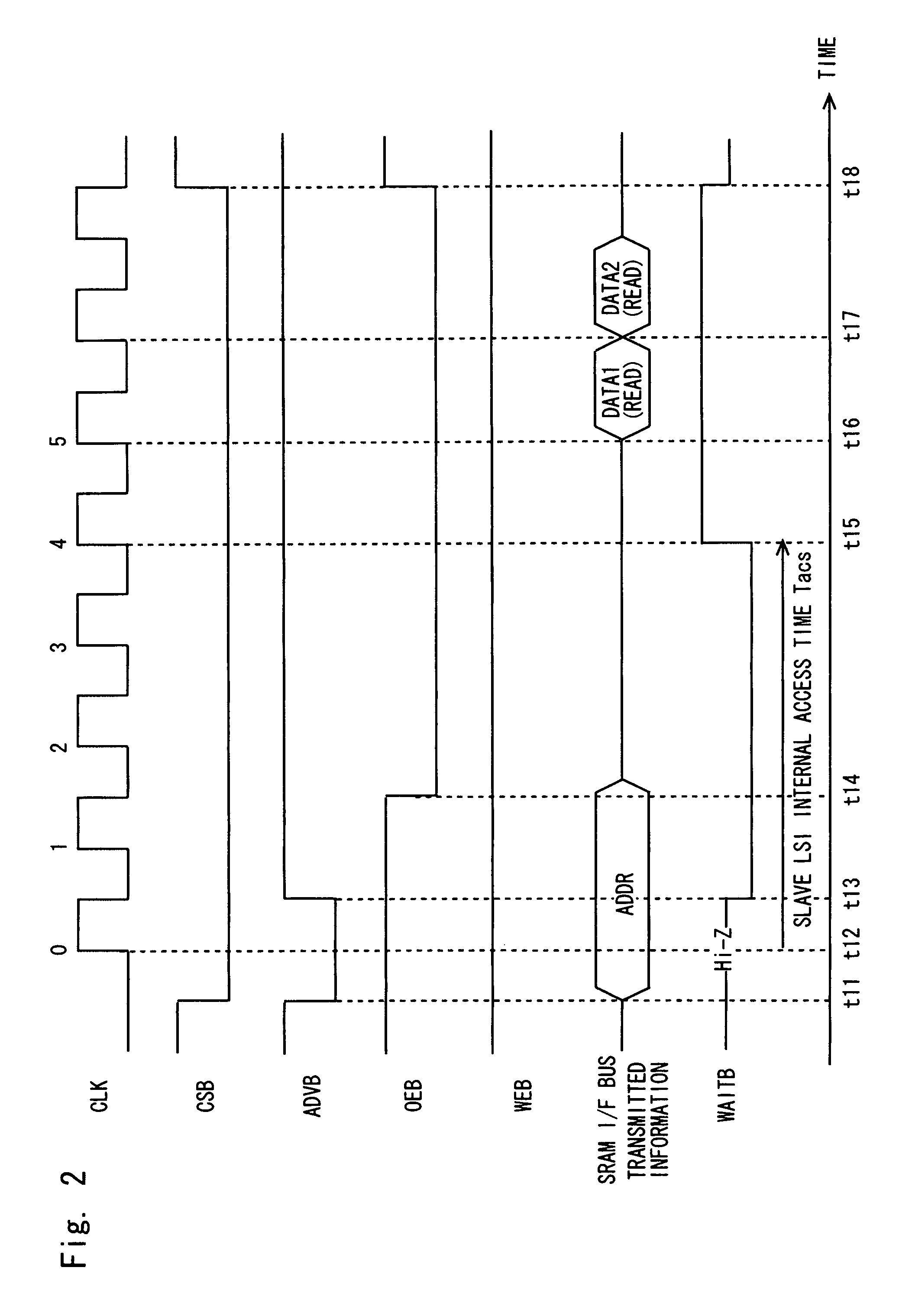
[0092]FIGS. 4 and 5 show timing charts to explain the internal operation of the slave LSI 120 of the information processing system 100 according to the second exemplary embodiment. First, FIG. 4 is a timing chart to explain the operation in which memory data under the slave LSI 120 is read by an access from the master LSI 110.

[0093]The chip select signal CSB is a signal for controlling the s...


PUM


Abstract

A control method of an information processing system including an address / data bus, the control method including: asserting a write enable signal indicating a write operation no later than an assertion of a latch control signal indicating an address latch timing in the write operation; asserting an output enable signal indicating a read operation after the address latch timing in the read operation; determine whether the write enable signal is asserted when the latch control signal is asserted; and starting the read or write operation according to the determined result no later than the address latch timing.

Description

INCORPORATION BY REFERENCE[0001]This application is based upon and claims the benefit of priority from Japanese patent application No. 2009-232541, filed on Oct. 6, 2009, the disclosure of which is incorporated herein in its entirety by reference.BACKGROUND[0002]1. Field of the Invention[0003]The present invention relates to an information processing system and a control method of the same.[0004]2. Description of Related Art[0005]FIG. 8 shows a block configuration of an information processing system 1 that is connected using an SRAM interface bus. Referring to FIG. 8, the information processing system 1 includes a master LSI 10, a slave LSI 20, ROM 30, and an SRAM interface bus 40.[0006]The master LSI 10, the slave LSI 20 and the ROM 30 are connected to the SRAM interface bus 40. The SRAM interface bus 40 is an AD-mux SRAM interface bus in which an address signal and a data signal are transmitted through a common bus line. Various control signals, the address signal and the data sig...

Claims


Application Information

Patent Timeline
Patent Type & Authority Patents(United States)
IPC IPC(8): G06F13/16G06F13/42G06F13/00G06F12/00
CPCG06F13/4217
Inventor KAZAMA, ATSUSHI
Owner RENESAS ELECTRONICS CORP
Why Eureka
Try Eureka