High-voltage semiconductor device with electrostatic discharge protection

a high-voltage semiconductor and protection technology, applied in the direction of semiconductor devices, electrical devices, transistors, etc., can solve the problems of electrical device malfunction and damage to the internal circuit, and achieve the effect of effectively introducing static charges and saving the cost of manufacturing the esd protection devi

Active Publication Date: 2013-05-07
UNITED MICROELECTRONICS CORP
View PDF23 Cites 2 Cited by
  • Summary
  • Abstract
  • Description
  • Claims
  • Application Information

AI Technical Summary

Benefits of technology

[0007]It is therefore a primary objective of the present invention to provide a high-voltage semiconductor device to prevent the internal circuit from being damaged by the ESD event generated from the input pad.
[0010]The high-voltage semiconductor device of the present invention integrates the ESD protection device and the depletion mode HV MOS transistor to effectively introduce the static charges from the first drain to the ground. Thus, the internal circuit electrically connected to the first source can be protected. In addition, the N-type second doped region of the high-voltage semiconductor device in the present invention serves as the second drain and the first source together, and thus, the cost of manufacturing the ESD protection device can be effectively saved.

Problems solved by technology

However, electrostatic discharge event easily occurs in the input end of the power conversion circuit that is directly electrically connected to the electrical power system, and the static charges enter into the internal circuit through the power conversion circuit, so that the internal circuit would be damaged by the static charges, and the electrical device malfunctions.

Method used


Image

  • High-voltage semiconductor device with electrostatic discharge protection
  • High-voltage semiconductor device with electrostatic discharge protection
  • High-voltage semiconductor device with electrostatic discharge protection

Examples


Embodiment Construction

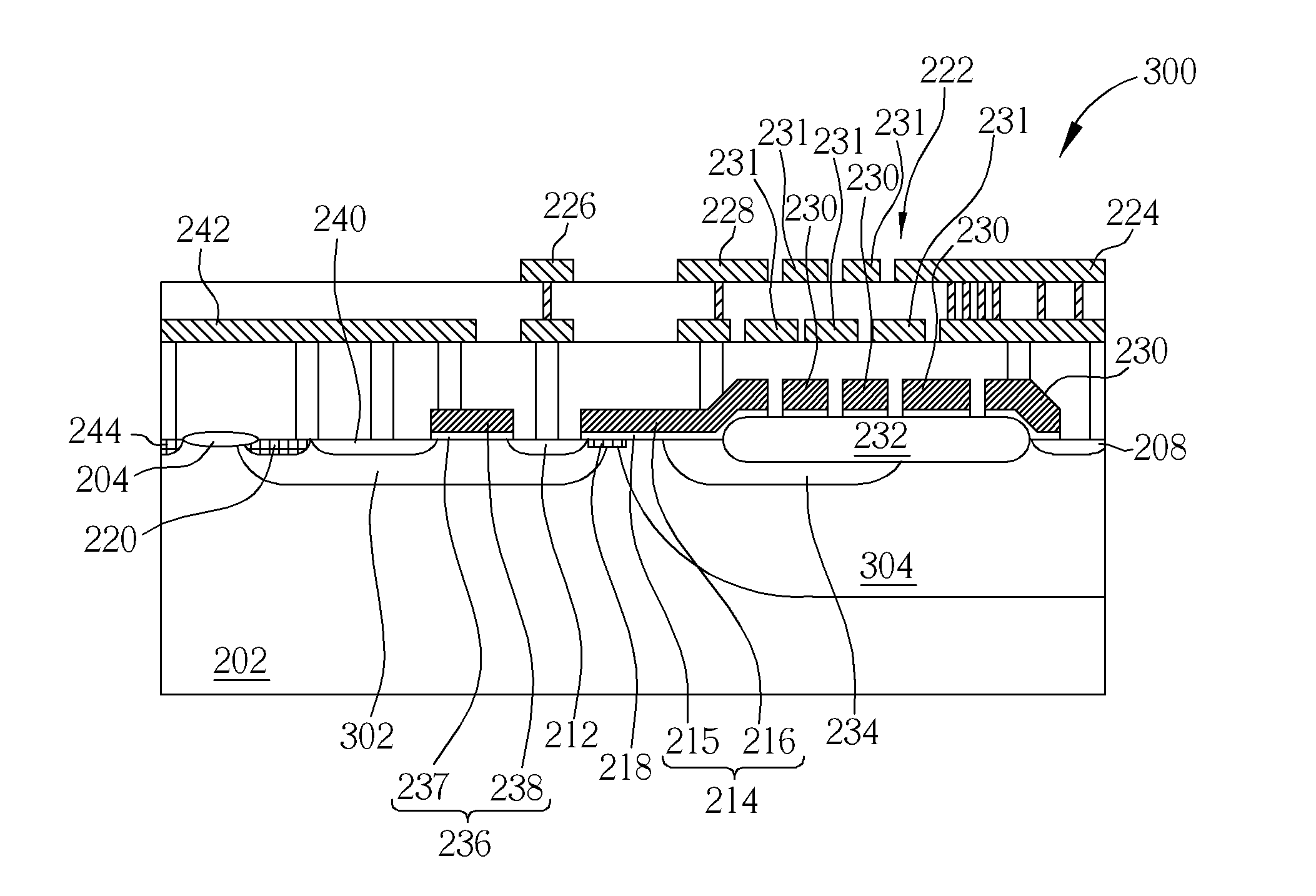
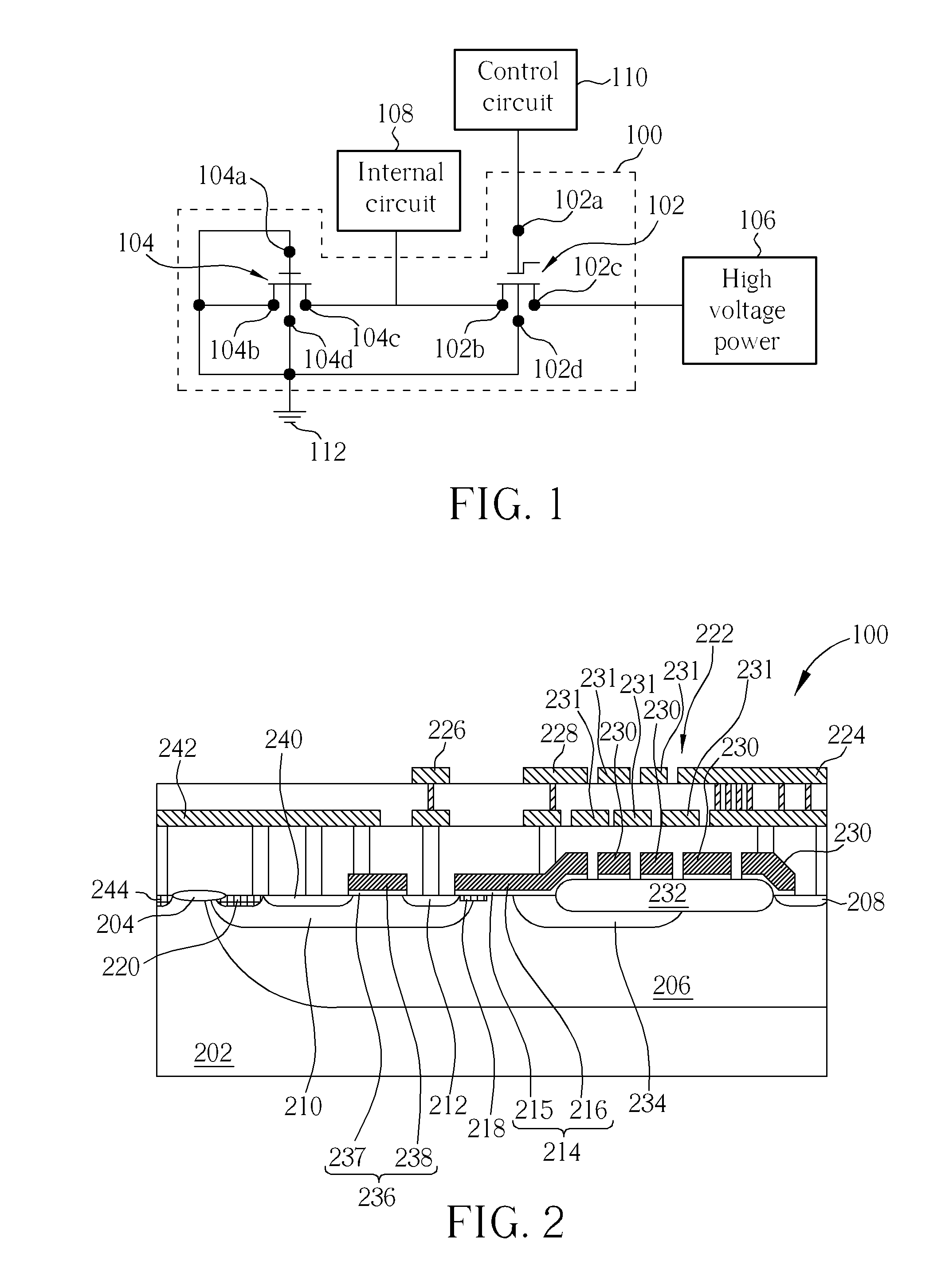
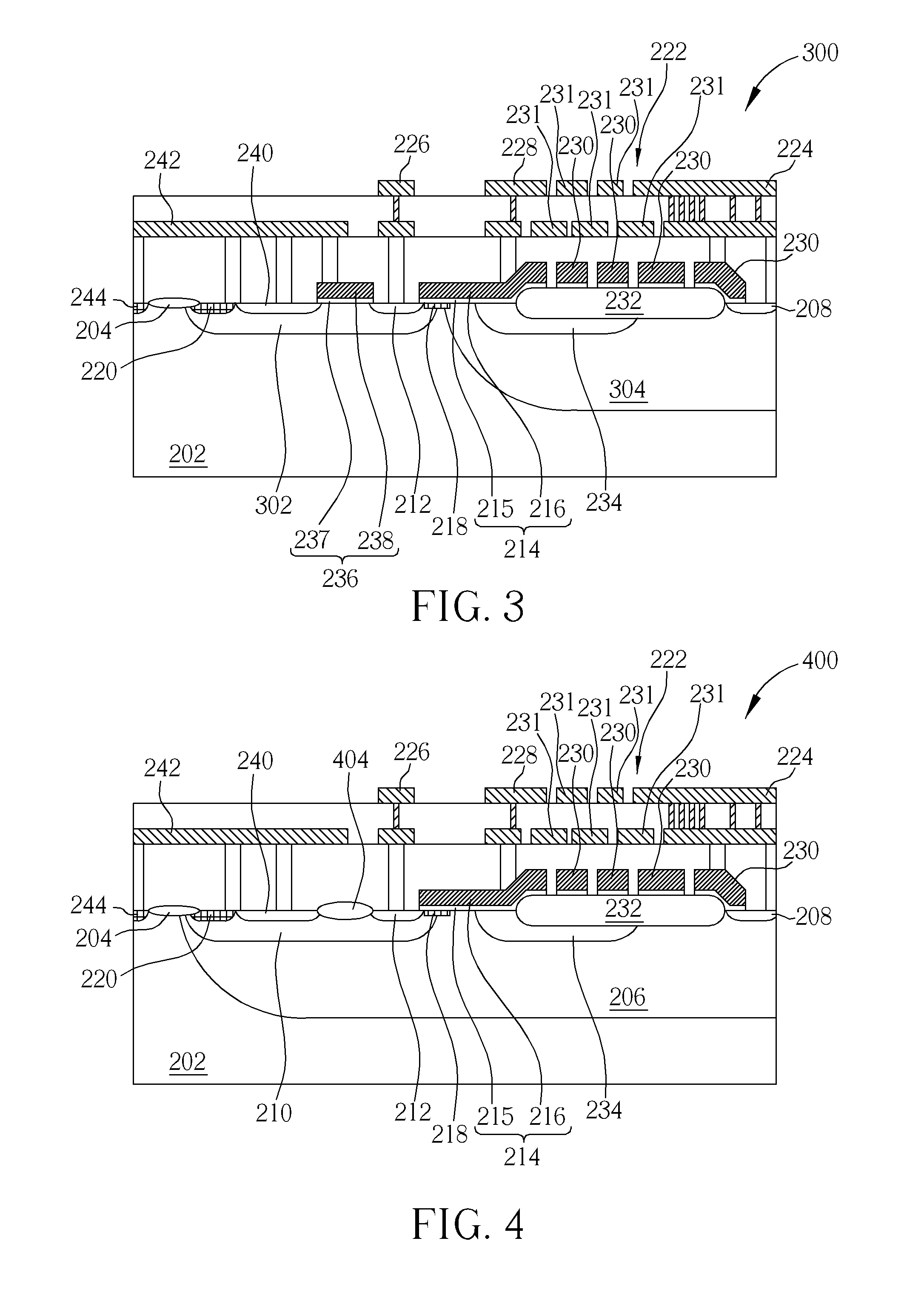
[0017]To provide a better understanding of the present invention, preferred embodiments will be detailed as follows. The preferred embodiments of the present invention are illustrated in the accompanying drawings with numbered elements to elaborate the contents and effects to be achieved.

[0018]Refer to FIG. 1, and FIG. 1 is a circuit diagram illustrating a high-voltage semiconductor device according to a first preferred embodiment of the present invention. As shown in FIG. 1, the high-voltage semiconductor device 100 includes a high-voltage metal-oxide-semiconductor (HV MOS) transistor 102, and an electrostatic discharge (ESD) protection device 104. The HV MOS transistor 102 has a first gate 102a, a first source 102b, a first drain 102c, and a first base 102d. The first drain 102c is electrically connected to a high-voltage power 106, such as a super high-voltage power providing 500 volts to 800 volts, and the first source 102b is electrically connected to an internal circuit to pro...


PUM


Abstract

The present invention provides a high-voltage semiconductor device including a deep well, a first doped region disposed in the deep well, a high-voltage well, a second doped region disposed in the high-voltage well, a first gate structure disposed on the high-voltage well between the second doped region and the first doped region, a doped channel region disposed in the high-voltage region and in contact with the second doped region and the deep well, and a third doped region disposed in the high-voltage well. The high-voltage well has a first conductive type, and the deep well, the first doped region, the second doped region, the doped channel region, and the third doped region have a second conductive type different from the first conductive type.

Description

BACKGROUND OF THE INVENTION[0001]1. Field of the Invention[0002]The present invention relates to a high-voltage semiconductor device, and more particularly, to a high-voltage semiconductor device integrating a high-voltage metal-oxide-semiconductor transistor with an electrostatic discharge protection device.[0003]2. Description of the Prior Art[0004]Current electrical power systems provide an alternating current having a variety of frequencies ranging from 50 to 60 Hz, and a voltage ranging from 100 volts to 240 volts, and with the differences of the electrical devices, operating voltage and frequencies also different. Thus, in order to provide a voltage corresponding to the operating voltage range of an electrical device, electrical device generally has a power conversion circuit disposed therein or at the outside thereof to electrically connect to the electrical power system, and a high voltage generated by the electrical power system can be reduced by the power conversion circui...

Claims


Application Information

Patent Timeline
Patent Type & Authority Patents(United States)
IPC IPC(8): H01L29/94
CPCH01L27/0251H01L27/0266H01L29/7835H01L29/7838H01L29/7817H01L29/404H01L29/42368H01L29/1087H01L29/861H01L29/0634
Inventor WANG, CHIH-CHUNGHSU, WEI-LUNWU, TE-YUANLIN, KE-FENGHUANG, SHAN-SHILEE, MING-TSUNGLEE, WEN-FANG
Owner UNITED MICROELECTRONICS CORP
Why Eureka
Try Eureka