CMOS-MEMS switch structure
a switch structure and micro-electromechanical technology, applied in the direction of contacts, relays, contact engagements, etc., can solve the problems of the switch structure b>100/b> still has many problems to be solved
- Summary
- Abstract
- Description
- Claims
- Application Information
AI Technical Summary
Benefits of technology
Problems solved by technology
Method used
Image
Examples
Embodiment Construction
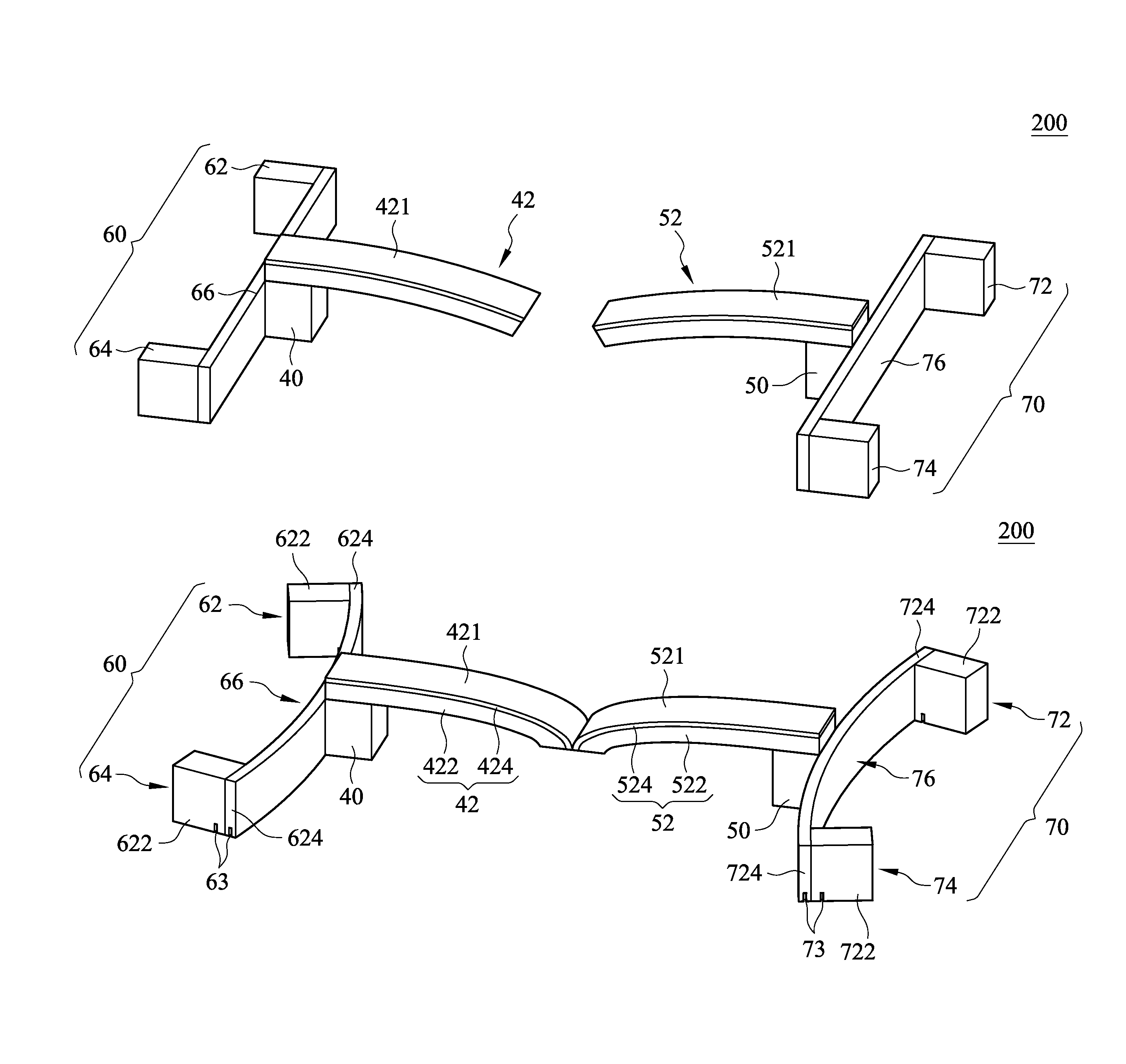
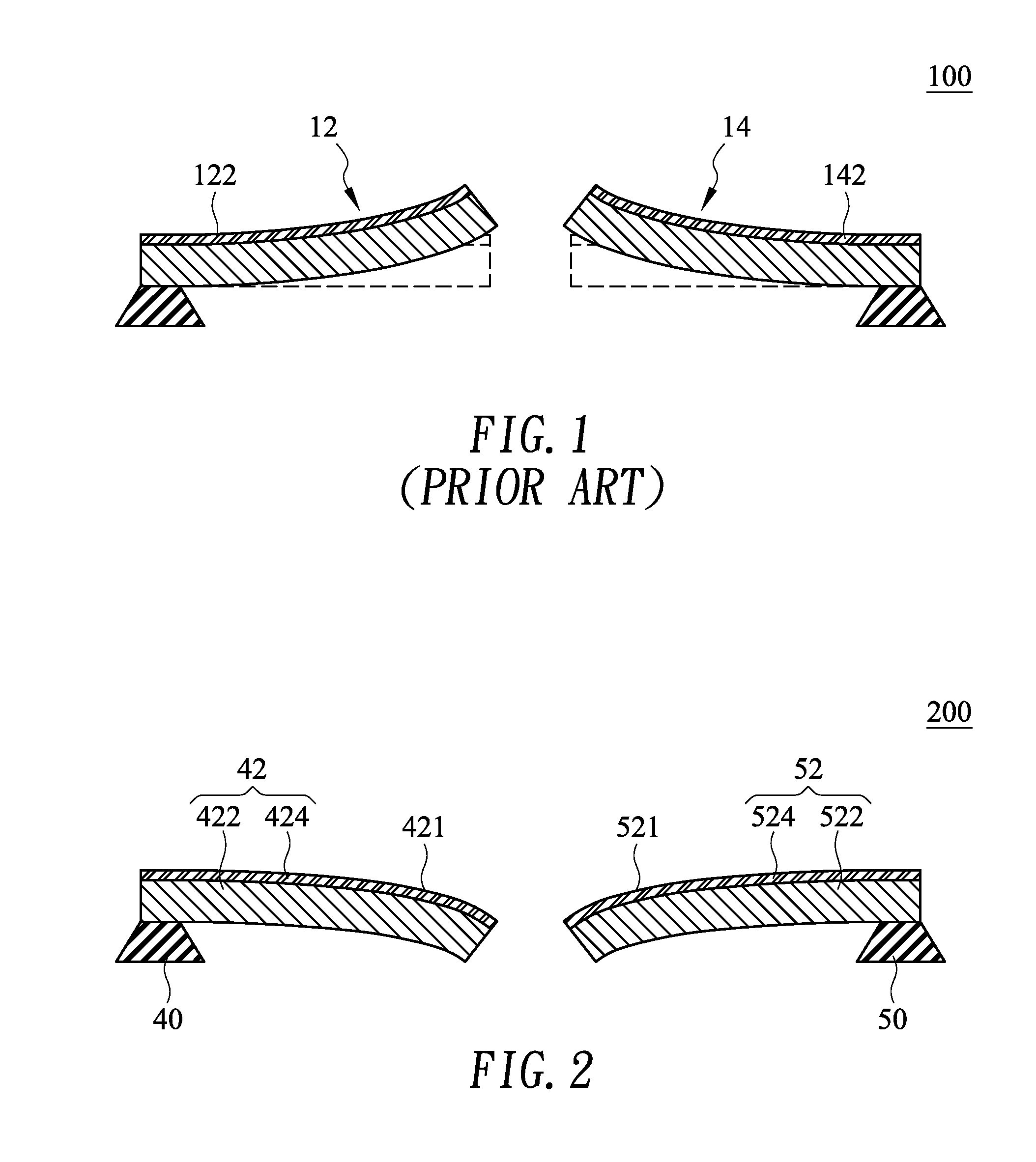
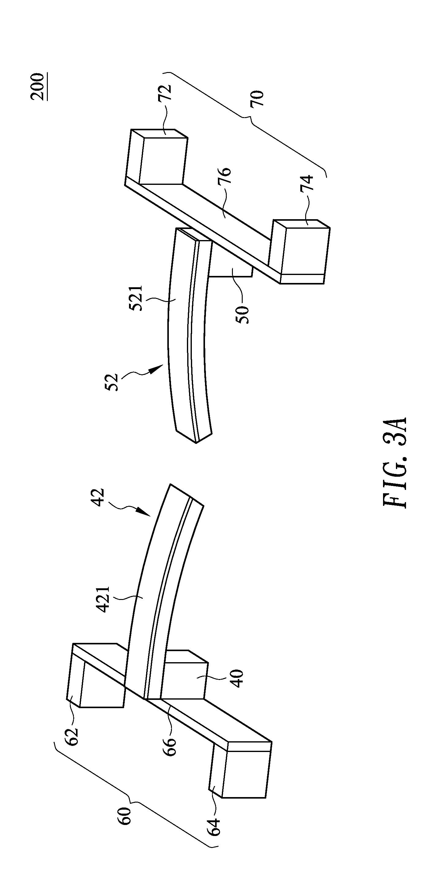
[0023]Referring to FIG. 2, a CMOS-MEMS switch structure 200 according to an embodiment of the present invention includes a first substrate 40, a second substrate 50, a first cantilever beam 42, and a second cantilever beam 52. The CMOS-MEMS switch structure 200 is made by a process incorporating both CMOS and MEMS manufacturing processes. For example, different layers of metals and oxides are stacked up using a standard 0.35-micron CMOS process. Then, MEMS element areas are defined on the stacked layers. Once the sacrificial layer arranged in the MEMS element areas is removed by etching, the desired MEMS structures are released. As the integrated CMOS-MEMS manufacturing processes have been developed to a very mature level, a detailed explanation of such processes is omitted, and only the resultant structure is described herein. It should be noted that all the materials of the disclosed CMOS-MEMS switch structure 200 are materials generally used in an integrated CMOS-MEMS manufacturi...
PUM
 Abstract
Description
Claims
Application Information


