Fully parameterizable representation of a higher level design entity

a design entity and fully parameterized technology, applied in the field of semiconductor analog circuits, can solve the problems of preventing the use of standardized cells and impeded the level of analog function design

Active Publication Date: 2013-06-11
BELL SEMICON LLC
View PDF9 Cites 1 Cited by
  • Summary
  • Abstract
  • Description
  • Claims
  • Application Information

AI Technical Summary

Problems solved by technology

The creation and placement of these individual electronic components, such as transistors, resistors and capacitors along with their metal interconnects provide a significant design challenge.
This level of design for analog functions has been impeded, since analog design involves specific tailoring of their components to meet design requirements thereby preventing the use of standardized cells.

Method used


Image

  • Fully parameterizable representation of a higher level design entity
  • Fully parameterizable representation of a higher level design entity
  • Fully parameterizable representation of a higher level design entity

Examples


Embodiment Construction

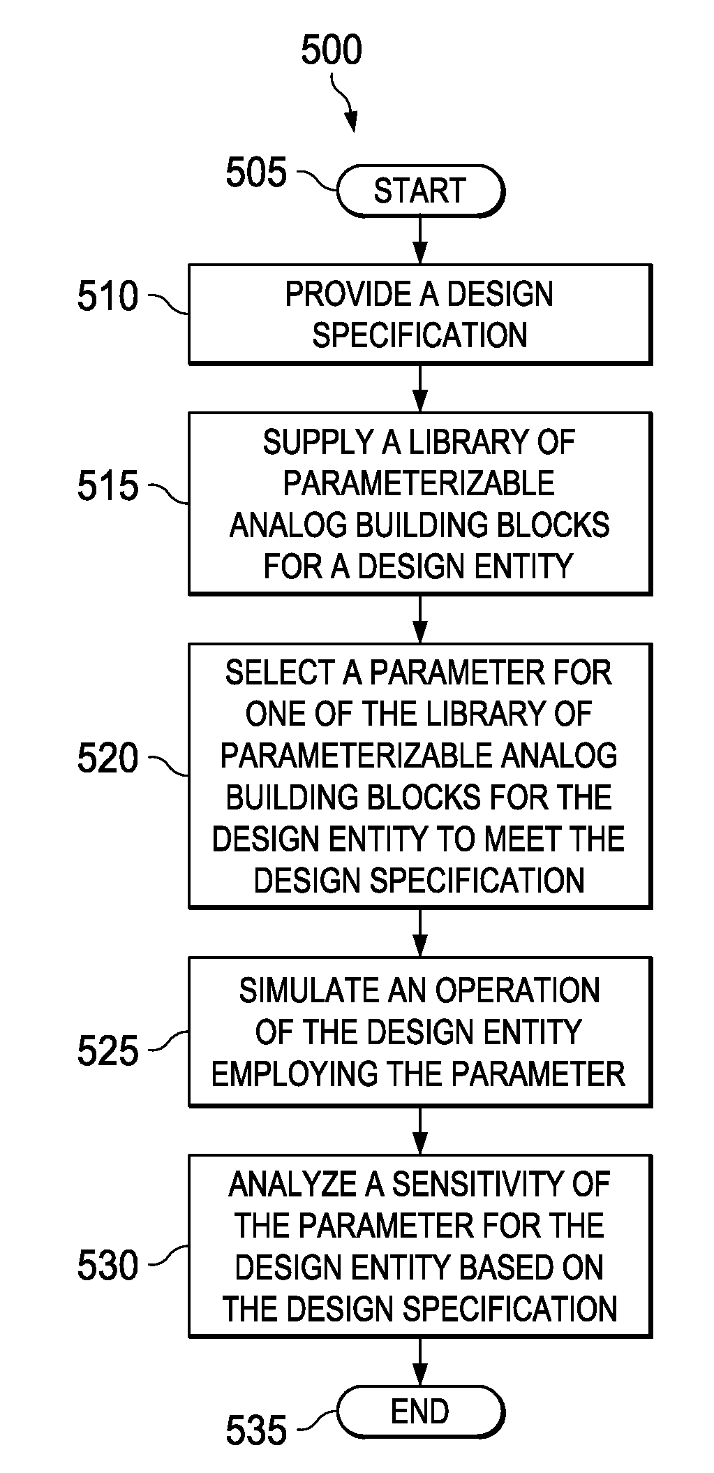
[0012]Embodiments of the present disclosure allow designing an analog circuit by piecing together parameterized higher level blocks instead of designing at a lower primitive level (i.e., a circuit component level). Furthermore, implementation is such that representations of a given higher level block, which may include device symbols, circuit diagrams, and mask layout drawings, are fully parameterized. This simplifies designing in advanced silicon technologies by freeing a designer from having to know a great deal about underlying technology restrictions, since parameterization is provided automatically through use of a parameterizable cell-based analog design methodology employing these fully parameterized representations. Embodiments of the disclosure may accommodate a wide range of variation across all aspects of the design process through this parameterization.

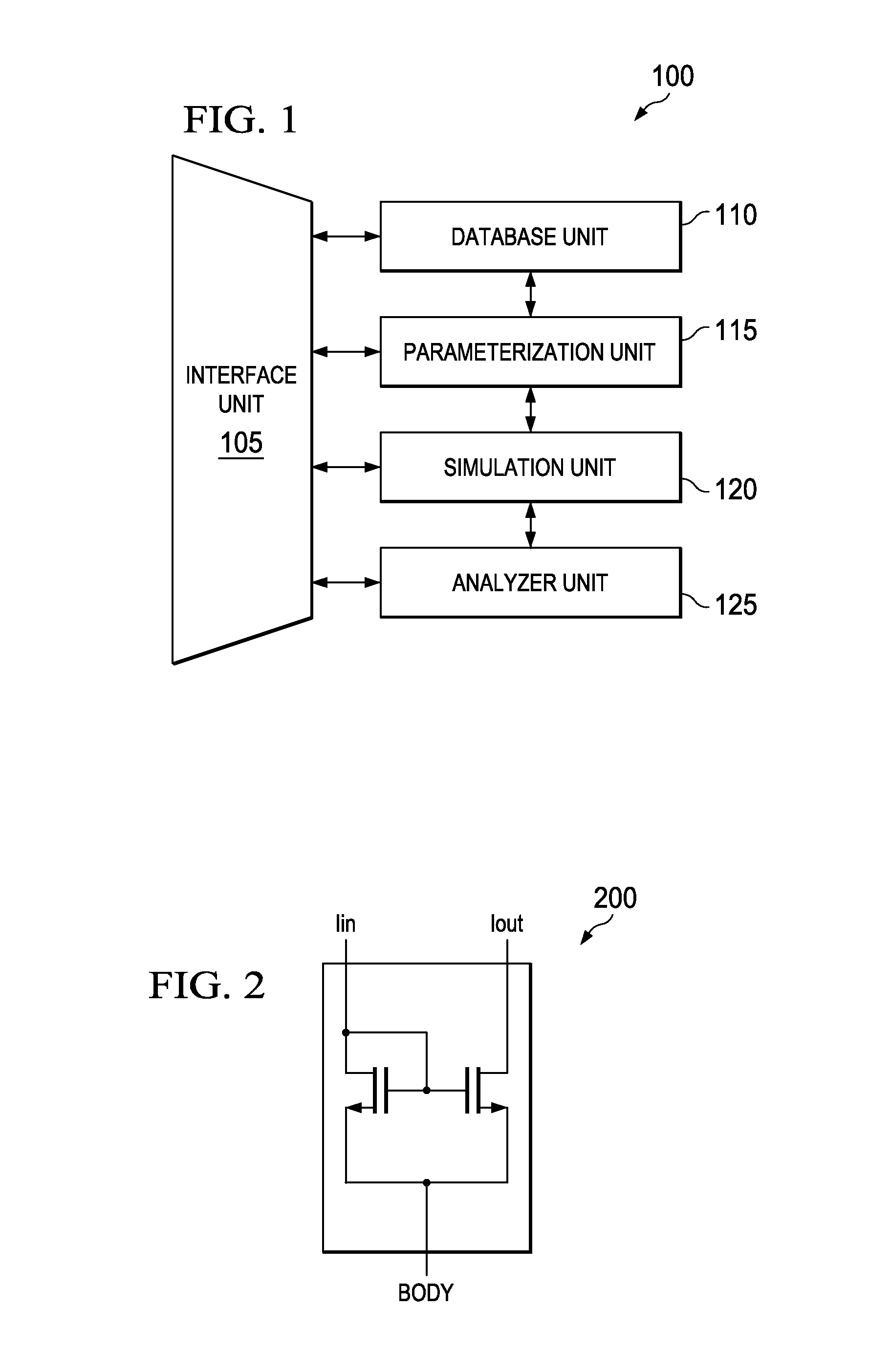
[0013]FIG. 1 illustrates a block diagram of an embodiment of a parameterizable design system, generally designated 100, ...


PUM


Abstract

A parameterizable design system is for use with semiconductor analog circuits and includes an interface unit connected to provide access to the system, a database unit connected to supply a library of parameterizable analog building blocks for a design entity, and a parameterization unit connected to select a parameter for one of the library of parameterizable analog building blocks to meet a design specification of the design entity. Additionally, the parameterizable design system may also include a simulation unit connected to simulate an operation of the design entity employing the parameter, and an analyzer unit connected to analyze a sensitivity of the parameter for the design entity based on the design specification. A method of designing a semiconductor analog circuit is also included.

Description

TECHNICAL FIELD[0001]This application is directed, in general, to semiconductor circuits and, more specifically, to a parameterizable design system and a method of designing a semiconductor analog circuit.BACKGROUND[0002]Generally, integrated circuits can employ millions of individual circuits to perform digital or analog functions. In turn, each of these individual circuits can employ hundreds, if not thousands, of individual electronic components. The creation and placement of these individual electronic components, such as transistors, resistors and capacitors along with their metal interconnects provide a significant design challenge. Computer aided design environments for digital functions have taken advantage of logic functions lending themselves to cell-based design approaches where the logic functions may be constructed of standardized cells. This level of design for analog functions has been impeded, since analog design involves specific tailoring of their components to mee...

Claims


Application Information

Patent Timeline
Patent Type & Authority Patents(United States)
IPC IPC(8): G06F17/50
CPCG06F17/5036G06F17/5063G06F2217/66G06F30/36G06F30/367G06F2115/08
Inventor BOSHART, SHAWNMOINIAN, SHAHRIARWILLIAMS, JOSHUAVUONG, HONG-HA
Owner BELL SEMICON LLC
Why Eureka
Try Eureka