Method of inspecting defect for electroluminescence display apparatus, defect inspection apparatus, and method of manufacturing electroluminescence display apparatus using defect inspection method and apparatus

a technology of defect inspection and display apparatus, applied in lighting and heating apparatus, semiconductor/solid-state device testing/measurement, instruments, etc., can solve problems such as unestablished efficient inspection methods, and achieve the effect of precisely and efficiently performing defect inspection of el display apparatus

Active Publication Date: 2013-07-23
SEMICON COMPONENTS IND LLC
View PDF24 Cites 74 Cited by
  • Summary
  • Abstract
  • Description
  • Claims
  • Application Information

AI Technical Summary

Benefits of technology

[0010]An advantage of the present invention is that a defect inspection of an EL display apparatus is executed precisely and efficiently.
[0011]According to one aspect of the present invention, there is provided a method of inspecting a defect for an electroluminescence display apparatus, wherein the display apparatus comprises, in each pixel, an electroluminescence element and an element driving transistor which is connected to the electroluminescence element and which controls a current flowing through the electroluminescence element, an inspection ON display signal which sets the electroluminescence element to an emission level is supplied to each pixel, the element driving transistor is operated in a saturation operating region of the transistor, an emission state of the electroluminescence element is observed, and a pixel having an emission brightness which is smaller than a reference brightness is detected as an abnormal display defect pixel, an inspection ON display signal which sets the electroluminescence element to an emission level is supplied to each pixel, the element driving transistor is operated in a linear operating region of the transistor, an emission state of the electroluminescence element is observed, and a non-emission pixel is detected as a dark spot defect pixel caused by the electroluminescence element, and a pixel which is detected as the abnormal display defect pixel and which is not detected as the dark spot defect pixel is detected as a dim spot defect pixel caused by the element driving transistor.
[0012]According to another aspect of the present invention, there is provided a method of inspecting a defect for an electroluminescence display apparatus, wherein the display apparatus comprises, in each pixel, an electroluminescence element having a diode structure and an element driving transistor which is connected to the electroluminescence element and which controls a current flowing through the electroluminescence element, an inspection ON display signal which sets the electroluminescence element to an emission level is supplied to each pixel, the element driving transistor in each pixel is operated in a linear operating region of the transistor, a current flowing through the electroluminescence element is detected, and a pixel is determined as a dark spot defect pixel caused by the electroluminescence element when a value of the current flowing through the electroluminescence element is greater than a predetermined value.
[0013]In the defect inspection method according to various aspects of the present invention, by executing the detection of the dark spot defect pixel after a reverse bias voltage is applied to the electroluminescence element of each pixel, it is possible to execute the dark spot defect inspection after screening the dark spot.
[0014]According to another aspect of the present invention, there is provided a method of inspecting a defect for an electroluminescence display apparatus, wherein the display apparatus comprises, in each pixel, an electroluminescence element having a diode structure and an element driving transistor which is connected to the electroluminescence element and which controls a current flowing through the electroluminescence element, an inspection ON display signal which sets the electroluminescence element to an emission level is supplied to each pixel, the element driving transistor is operated in a saturation operating region of the transistor, and a current flowing through the electroluminescence element is detected, and a pixel is detected as a dim spot defect pixel caused by the element driving transistor when a value of the current flowing through the electroluminescence element is smaller than a predetermined value.
[0015]According to another aspect of the present invention, there is provided a defect inspection apparatus for an electroluminescence display apparatus which comprises, in each pixel, an electroluminescence element having a diode structure and an element driving transistor which is connected to the electroluminescence element and which controls a current flowing through the electroluminescence element, the defect inspection apparatus comprising a power supply generation section which generates a power supply to be supplied to each pixel during defect inspection, an inspection signal generation section which generates an inspection timing signal and an inspection ON display signal, a current detecting section which detects a current flowing through the electroluminescence element, and a defect determining section.

Problems solved by technology

On the other hand, regarding display unevenness (DIM) and dark spots, various causes are being found.
However, there had not been established an efficient method of inspection according to the cause of occurrence.

Method used


Image

  • Method of inspecting defect for electroluminescence display apparatus, defect inspection apparatus, and method of manufacturing electroluminescence display apparatus using defect inspection method and apparatus
  • Method of inspecting defect for electroluminescence display apparatus, defect inspection apparatus, and method of manufacturing electroluminescence display apparatus using defect inspection method and apparatus
  • Method of inspecting defect for electroluminescence display apparatus, defect inspection apparatus, and method of manufacturing electroluminescence display apparatus using defect inspection method and apparatus

Examples


Embodiment Construction

[0042]A preferred embodiment of the present invention (hereinafter referred to as “embodiment”) will now be described with reference to the drawings.

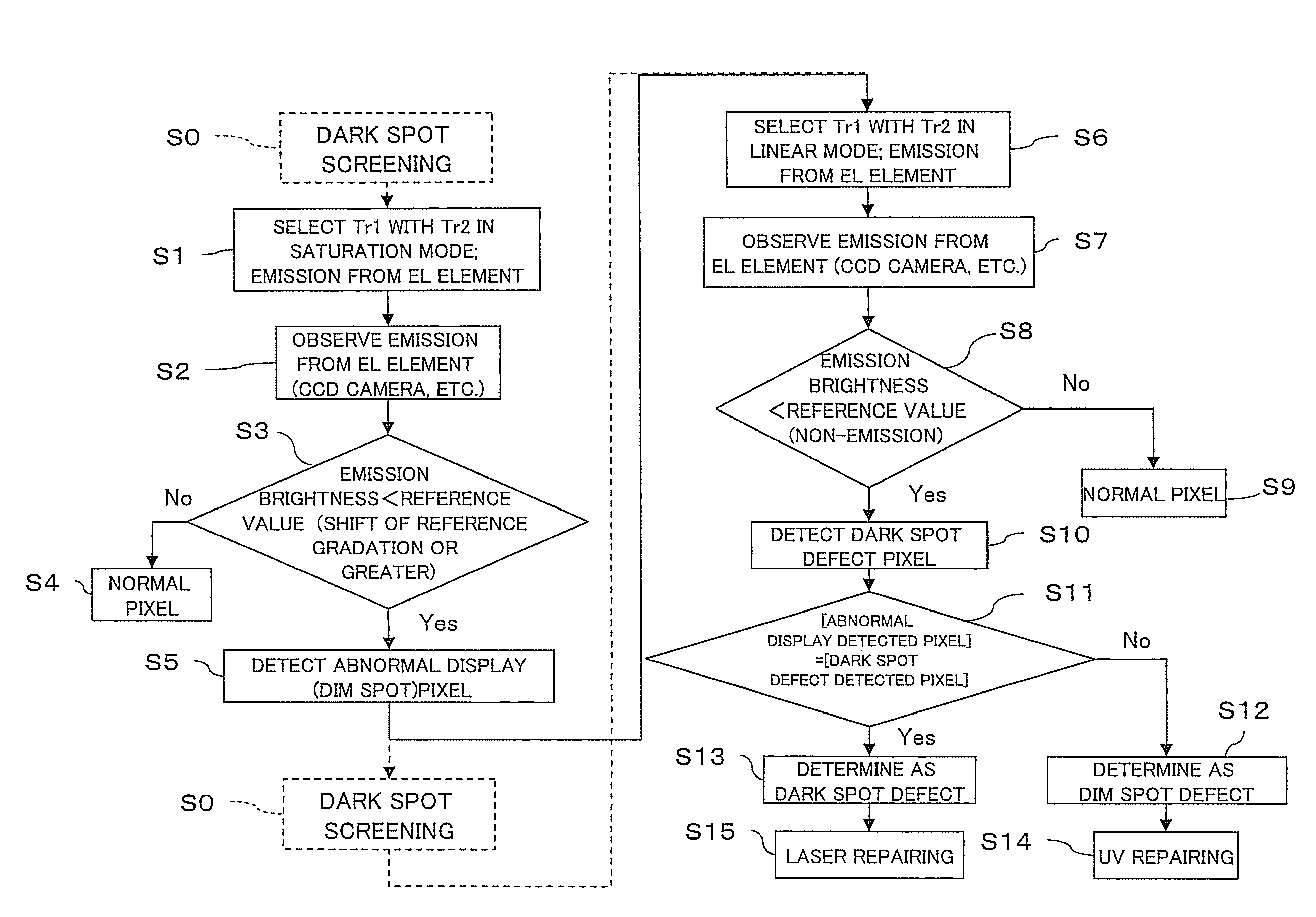
[0043][Inspection Principle]

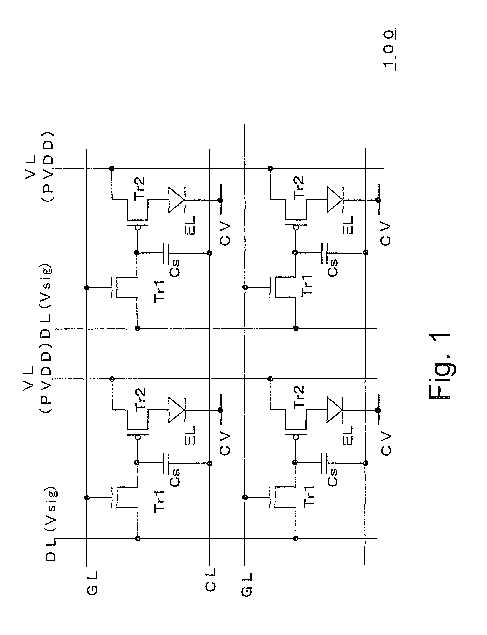
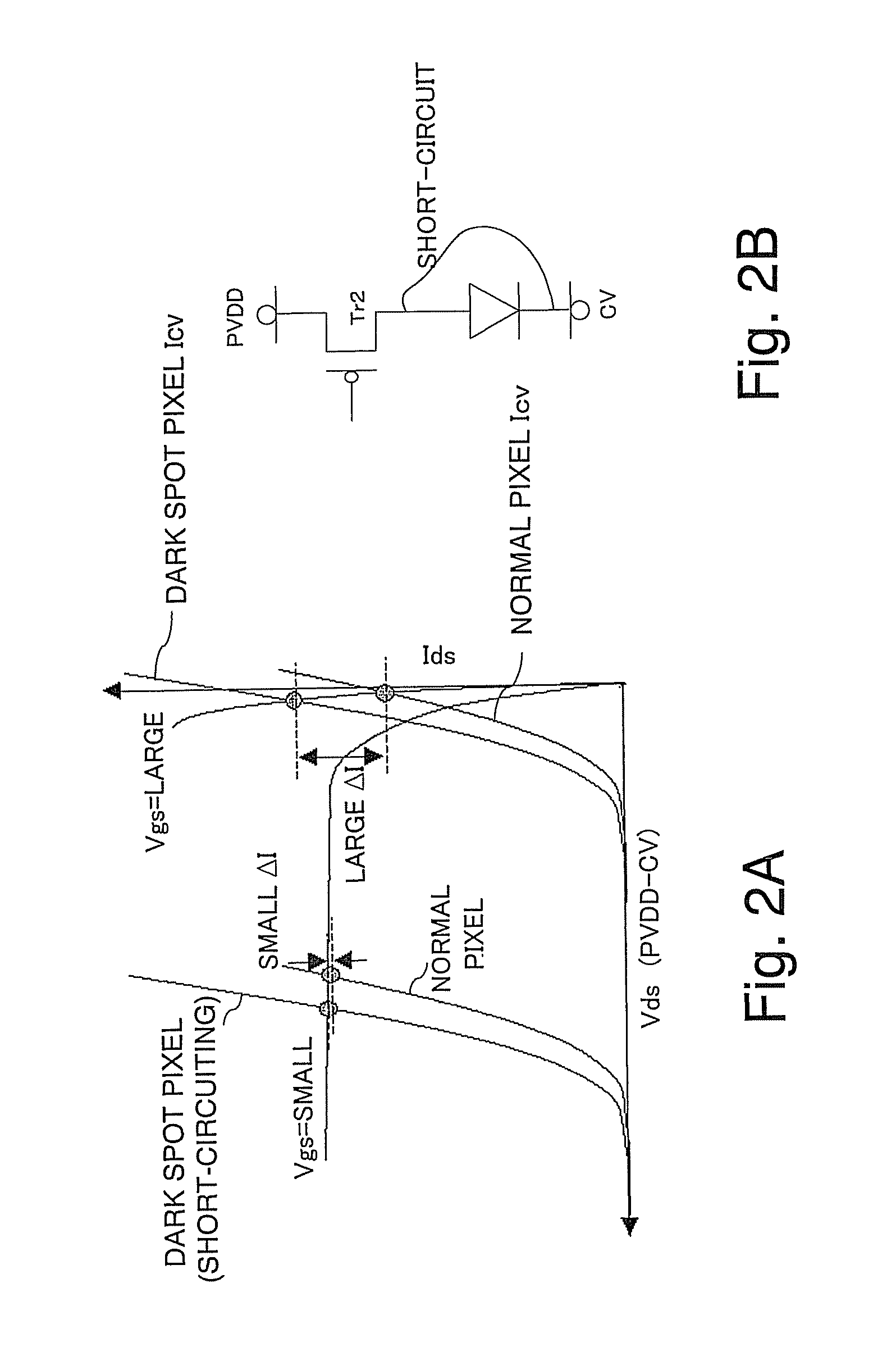
[0044]In the embodiment, a display apparatus is an active matrix organic electroluminescence (EL) display apparatus, and a display section having a plurality of pixels is formed on an EL panel 100. FIG. 1 is a diagram showing an equivalent circuit structure of an active matrix display apparatus according to the embodiment, and FIGS. 2 and 3 show a principle of defect inspection of the pixels of the EL display apparatus employed in the present embodiment. A plurality of pixels are arranged in the display section of the EL panel 100 in a matrix form, a selection line GL on which a selection signal is sequentially output is formed along a horizontal scan direction (row direction) of the matrix, and a data line DL on which a data signal is output and a power supply line VL for supplying a drive power supply PVDD ...


PUM

PropertyMeasurementUnit
voltageaaaaaaaaaa
voltageaaaaaaaaaa
bias voltages Vbiasaaaaaaaaaa

Abstract

A dark spot defect of an EL element is detected based on an emission brightness or a current flowing through the EL element when an element driving transistor which controls a drive current to be supplied to the EL element is operated in its linear operating region and the EL element is set to an emission level. A dim spot defect caused can be detected based on a current flowing through the EL element when the element driving transistor is operated in its saturation operating region and the EL element is set to the emission level. When an abnormal display pixel is detected based on an emission brightness, a pixel which is determined as an abnormal display pixel and which is not determined as a dark spot defect is determined, and the pixel is detected as a dim spot defect caused by the characteristic variation of the element driving transistor.

Description

CROSS-REFERENCE TO RELATED APPLICATIONS[0001]The entire disclosure of Japanese Patent Application No. 2006-239626 including specification, claims, drawings, and abstract is incorporated herein by reference.BACKGROUND OF THE INVENTION[0002]1. Field of the Invention[0003]The present invention relates to inspection of a defect caused by an electroluminescence element in a display apparatus having the electroluminescence element in each pixel or caused by a transistor which drives the electroluminescence element.[0004]2. Description of the Related Art[0005]Electroluminescence (hereinafter referred to as “EL”) display apparatuses in which an EL element which is a self-emissive element is employed as a display element in each pixel are expected as a flat display apparatus of the next generation, and are being researched and developed.[0006]After an EL panel is created in which an EL element and a thin film transistor (hereinafter referred to as “TFT”) or the like for driving the EL elemen...

Claims


Application Information

Patent Timeline
Patent Type & Authority Patents(United States)
IPC IPC(8): G09G3/32H05B33/10G01N21/95H01L21/66
CPCG09G3/006G09G3/3225G09G3/3233H05B33/10
Inventor OGAWA, TAKASHI
Owner SEMICON COMPONENTS IND LLC
Why Eureka
Try Eureka