Display device utilizing conductive adhesive to electrically connect IC substrate to non-display region and manufacturing method of the same

a technology of conductive adhesives and adhesives, which is applied in the direction of radio frequency controlled devices, instruments, optics, etc., can solve the problems of difficult to implement electroplating on glass substrates, inability to use ic formed on conventional semiconductor wafers, etc., and achieves improved uniformity, improved thickness of pad parts, and advantageous control of pressure conditions and the like

Active Publication Date: 2013-08-06
LG DISPLAY CO LTD
View PDF8 Cites 0 Cited by
  • Summary
  • Abstract
  • Description
  • Claims
  • Application Information

AI Technical Summary

Benefits of technology

[0028]The conventional liquid display device and the pad part and the fabricating method have following disadvantages.
[0053]According to the display device and the fabricating method, a bump is formed in a pad part of a first substrate (thin film layer transistor array substrate) of a display device and uniformity may be improved.
[0054]Furthermore, the height of the pad part may be increased stably. As a result, when an IC substrate is bonded with a display panel, a pressure condition and the like may be controllable advantageously.

Problems solved by technology

First of all, to attach a drive IC substrate or an IC substrate for a specific function manufactured in a low temperature poly silicon forming process to a display panel, it is impossible to use the IC formed on a conventional semiconductor wafer as it is.
It is difficult to implement the electroplating on a glass substrate because damage to the glass substrate might occur.

Method used


Image

  • Display device utilizing conductive adhesive to electrically connect IC substrate to non-display region and manufacturing method of the same
  • Display device utilizing conductive adhesive to electrically connect IC substrate to non-display region and manufacturing method of the same
  • Display device utilizing conductive adhesive to electrically connect IC substrate to non-display region and manufacturing method of the same

Examples


first embodiment

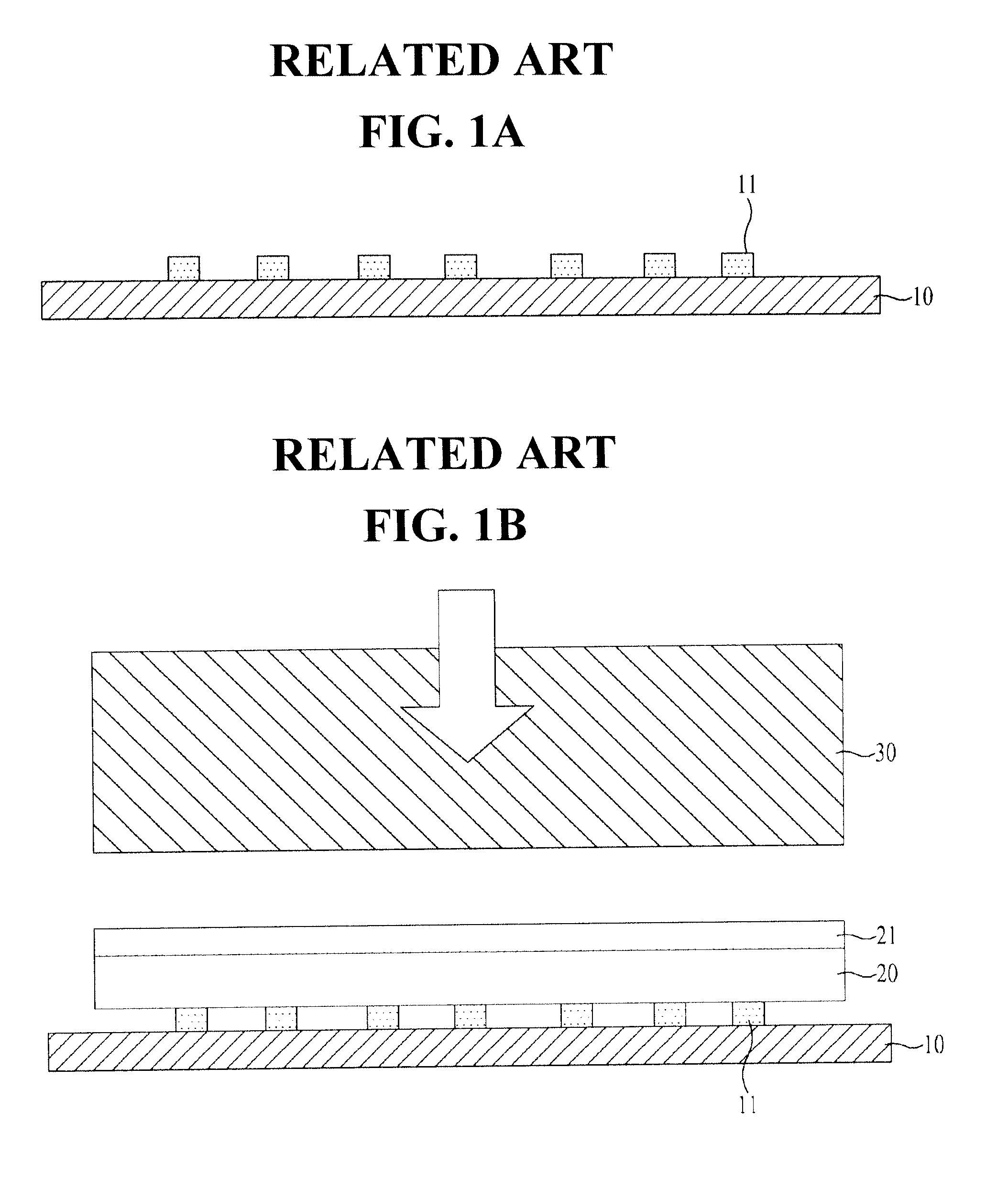
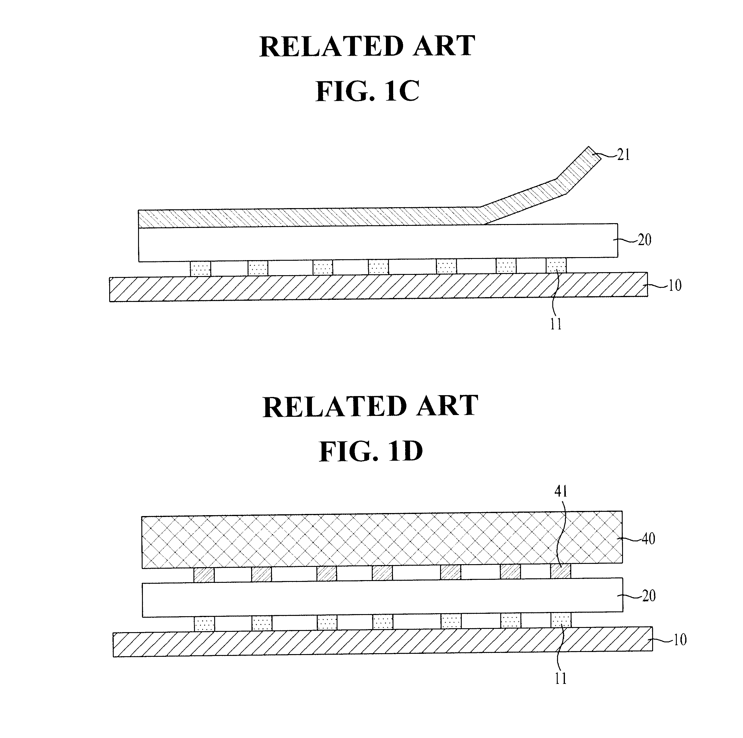
[0068]FIGS. 2A and 2B are sectional views illustrating an IC substrate and a substrate of a display device according to an embodiment of the pad part forming method.

[0069]In the pad part forming method according to an exemplary embodiment of the present invention, a first substrate 100 is prepared and a first buffer layer 110 is formed as shown in FIG. 2A.

[0070]Here, the first substrate 100 is made of glass and a pad part is an outer portion of one of both substrates bonded to each other to form a display panel.

[0071]Here, a portion shown in the drawing is corresponding to a pad region of the first substrate 100 in which a thin film layer transistor array is formed. An outer portion of the first substrate 100 having the thin film layer array formed therein may be larger than an outer portion of the second substrate (not shown) opposed to the first substrate 100 and this large portion defines a pad part to apply an electric signal.

[0072]Hence, a thin film layer transistor array (not ...

second embodiment

[0112]FIG. 4 is a diagram illustrating plane view illustrating a first substrate of a display device according to a pad part forming method of a display device according to a second embodiment of the present invention. FIG. 5 is a sectional view illustrating a structure along I˜I′ line shown in FIG. 4. FIG. 6 is a sectional view illustrating a forming state of the first substrate and a pad part of the display device based on the pad part forming method of the display device according to the second embodiment of the present invention.

[0113]As shown in FIGS. 4 and 5, the pad part forming method of the display device according to the second embodiment is implemented based on a following order.

[0114]First of all, a buffer layer 110 is formed on a first substrate 100.

[0115]Hence, a poly silicon dummy pattern 150 is formed in a predetermined area on the buffer layer 110. Depending on cases, the plurality of the poly silicon dummy patterns 150 may be formed in a metal pad electrode shape, ...


PUM


Abstract

A display device and a fabricating method of the same are disclosed. The display device includes a first substrate comprising a display region defined in a center thereof and a non-display region defined in an outer area thereof, the display region comprising a thin film layer transistor array and the non-display region comprising a pad electrode; an IC substrate opposed to a predetermined area of the non-display region; a circuit pad electrode formed on the IC substrate; a step pattern formed on the circuit pad electrode, the step pattern made of an organic dielectric layer; a circuit pad contact hole formed in the step pattern the to partially expose the circuit pad electrode; a transparent circuit pad electrode formed on the step pattern including the circuit pad contact hole; and a conductive adhesive formed between the first substrate and the IC substrate, the conductive adhesive comprising conductive balls to electrically connect the transparent circuit pad electrode and the pad electrode with each other.

Description

CROSS REFERENCE TO RELATED APPLICATION[0001]This application claims the benefit of the Patent Korean Application No. 10-2009-127943, filed on Dec. 21, 2009, which is hereby incorporated by reference as if fully set forth herein.BACKGROUND OF THE DISCLOSURE[0002]1. Field of the Disclosure[0003]The present invention relates to a display device, more particularly, to a display device which changes a structure of an IC substrate to gain an enough step, when bonding a drive IC fabricated by using LDIC technology with a substrate of the display device made of an IC substrate and a glass substrate, and a fabricating method of the same.[0004]2. Discussion of the Related Art[0005]As the information age has started in earnest, a display field used to express an electrical information signal visually has been developed drastically. Together with that, a variety of flat display devices having excellent functions of slimming, reduced weights and low electricity consumption has been developed and...

Claims


Application Information

Patent Timeline
Patent Type & Authority Patents(United States)
IPC IPC(8): H01L31/0203H01L31/18
CPCG02F1/1345G02F1/13452H01L2224/2939H01L2224/17107H01L23/3114H01L2224/05687H01L2224/2929H01L2224/83851H01L2924/01079H01L2924/3025H01L2224/29444H01L2224/05572H01L2224/29455H01L2924/0002H01L2224/0401H01L2924/0543H01L2924/00014H01L2224/05552H01L2924/12044H01L2924/00G02F1/13458
Inventor BAEK, MYOUNG-KEE
Owner LG DISPLAY CO LTD
Why Eureka
Try Eureka