
Organic electroluminescent device

a technology of electroluminescent devices and organs, which is applied in the manufacture of electrode systems, electric discharge tubes/lamps, and discharge tubes luminescent screens, etc., can solve the problems of non-emissive areas being brightened, and achieve the effect of preventing electrical shorts and improving light emission

Inactive Publication Date: 2013-08-13
KONINK PHILIPS ELECTRONICS NV
View PDF16 Cites 1 Cited by
  • Summary
  • Abstract
  • Description
  • Claims
  • Application Information

AI Technical Summary

Benefits of technology

The present invention provides an organic electroluminescent device with a spacer structure for preventing electrical shorts between both electrodes. The spacer means are less visible or invisible for the viewer of the device and comprise light scattering means for redirecting trapped light. The device shows a more homogeneous brightness distribution and better light emission. The scattering properties can be adapted to achieve a homogeneous brightness distribution with almost invisible spacer means. The device is more effective and visually appealing with a smaller number of spacer means.

Problems solved by technology

This results in a brightening of the otherwise non-emissive area.

Method used


Image

  • Organic electroluminescent device
  • Organic electroluminescent device
  • Organic electroluminescent device

Examples


Embodiment Construction

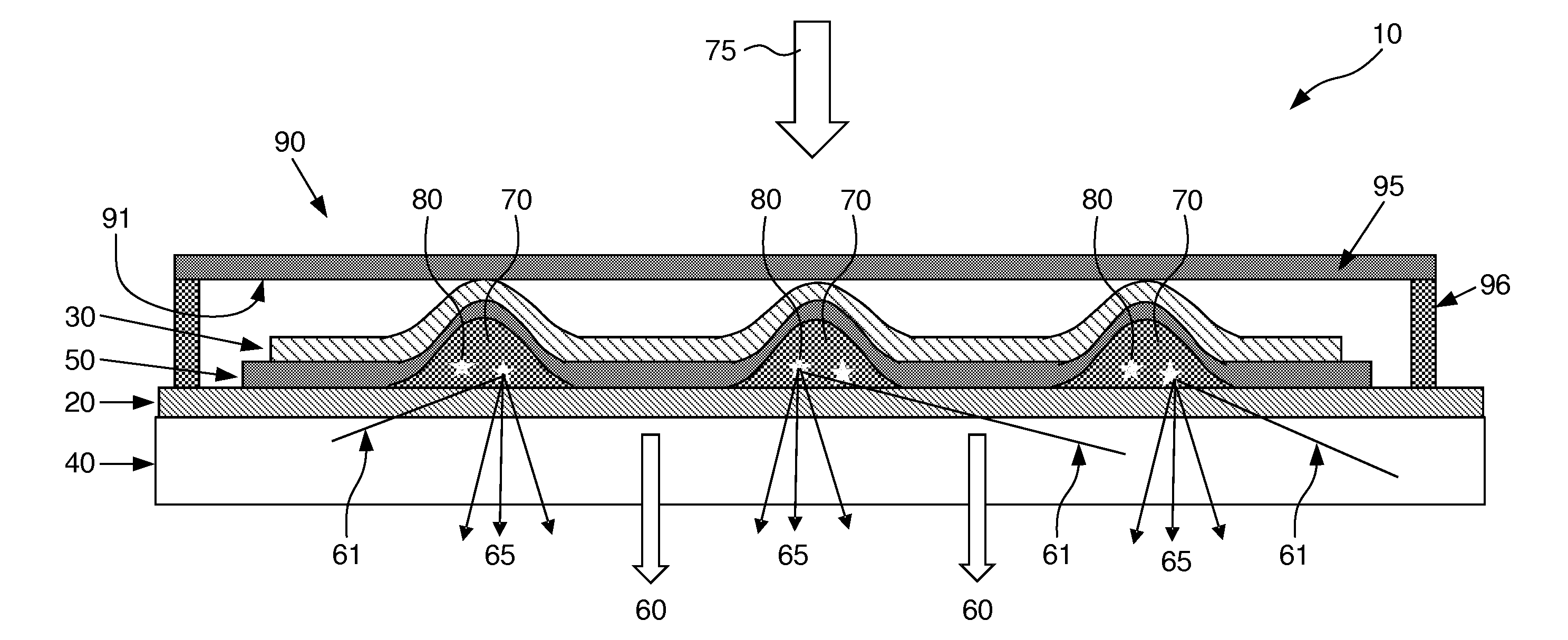
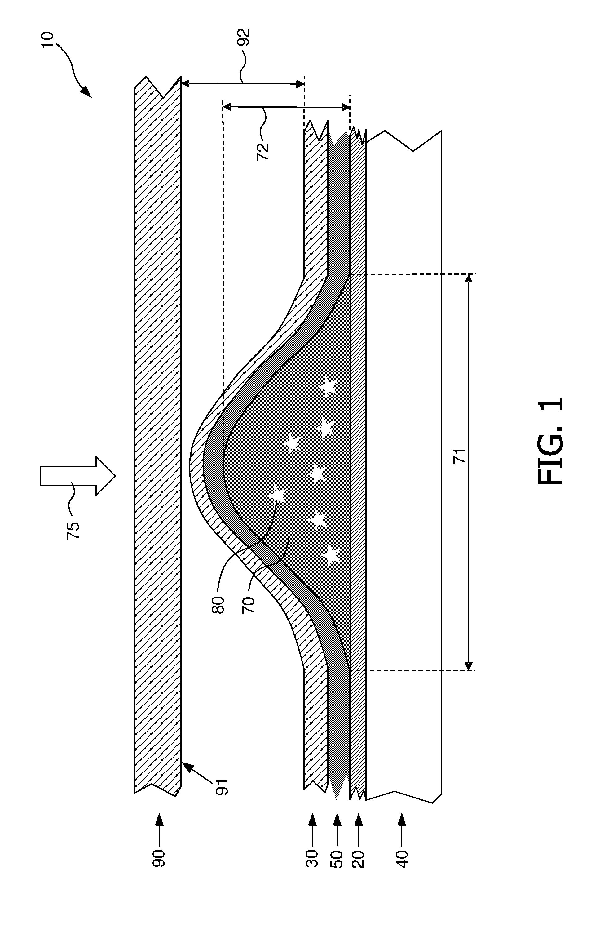
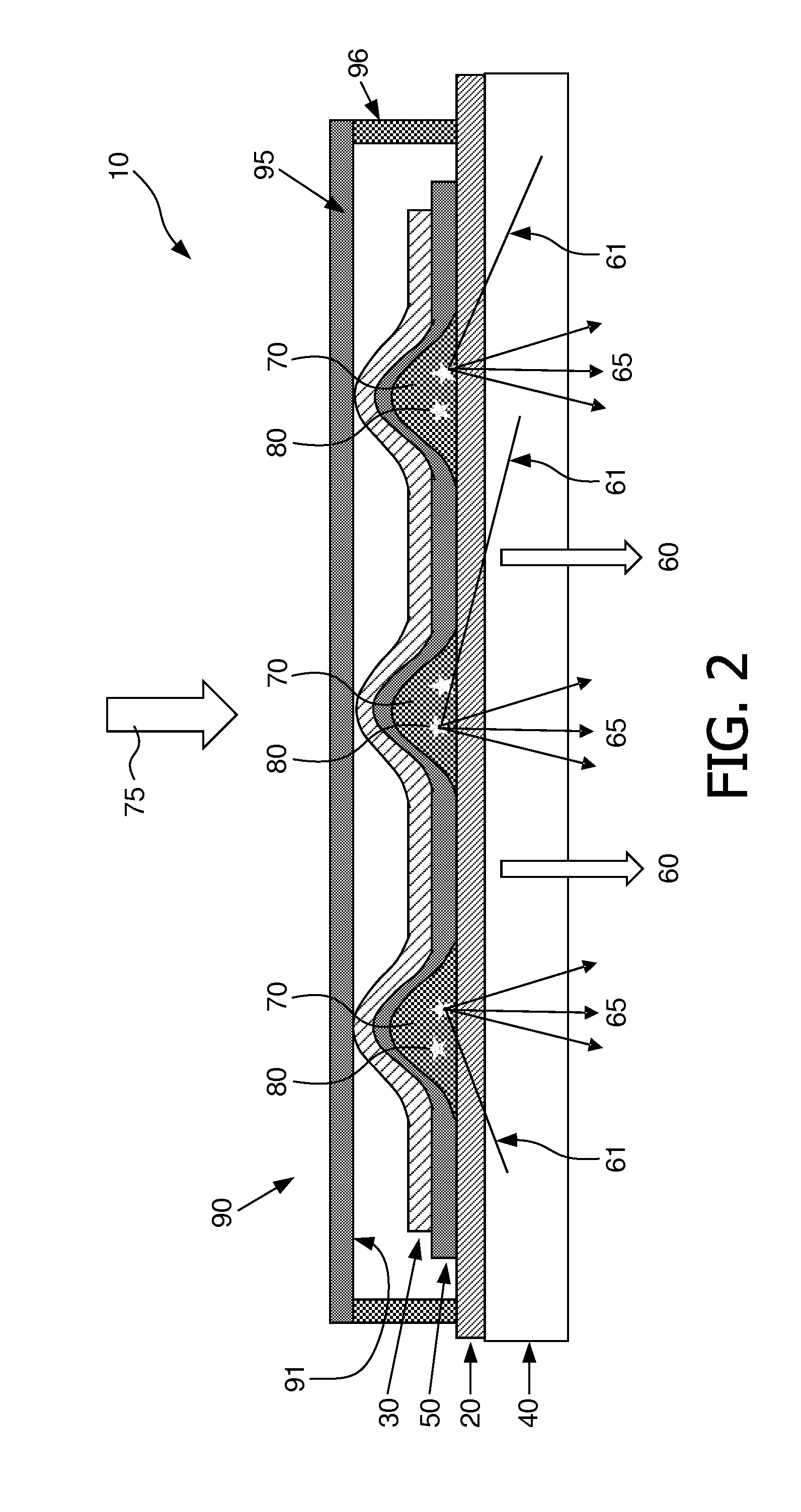
[0044]FIG. 1 shows an electroluminescent device 10 (OLED) according to the present invention comprising a substrate 40 and on top of the substrate a substrate electrode 20, a counter electrode 30, an electroluminescent layer stack 50 and an encapsulation means 90. The electroluminescent layer stack 50 is arranged between the substrate electrode 20 and the counter electrode 30 comprising at least one organic light emitting layer. The electroluminescent layer stack has a thickness of typically 100-200 nm. The substrate electrode 20 is formed by an approximately 100 nm thick layer of ITO, which is a transparent and conductive material. On top of the substrate electrode 20 a spacer means 70 comprising scattering particles as the scattering means 80. For example the scattering particles 80 may be Aluminum particles with diameters of about 1 micrometer. Onto the substrate electrode 20 and the spacer means 70, the organic electroluminescent layer 50 and subsequently the counter electrode 3...


PUM


Abstract

The present invention relates to an organic electroluminescent device comprising a substrate (40) and on top of the substrate (40) a substrate electrode (20), a counter electrode (30) and an electroluminescent layer stack (50) with at least one organic electroluminescent layer arranged between the substrate electrode (20) and the counter electrode (30), an encapsulation means (90) encapsulating at least the electroluminescent layer stack (50) and at least one non-conductive spacer means (70) arranged on the substrate electrode (20) to mechanically support the encapsulation means (90) and to prevent an electrical short between the substrate electrode (20) and the counter electrode (30) during the mechanical support, wherein the spacer means (70) comprise at least one light scattering means (80) for redirecting at least a part of light (65) trapped in the substrate (40), to a method of manufacturing such an encapsulated electroluminescent device and to the use of an array, preferably a hexagonal array, of non-conductive spacer means.

Description

FIELD OF THE INVENTION[0001]The present invention relates to an organic electroluminescent device encapsulated by an encapsulation means, a method of manufacturing such an encapsulated electroluminescent device and the use of an array of almost invisible spacer means to support the electroluminescent device.BACKGROUND OF THE INVENTION[0002]Common organic electroluminescent devices (OLEDs) comprise a functional layer stack on top of a substrate with at least one organic electroluminescent layer sandwiched between a substrate and a counter electrode, whereas parts of the electroluminescent layer and / or parts of the counter electrode are sensitive to water and / or oxygen. Therefore OLEDs are encapsulated by cover lids to prevent ambient substance such as water and oxygen from reaching the functional layers, to provide OLED devices having a sufficient lifetime. The cover lid defines an encapsulated volume around the functional layer stack with typically a gap or space between the outermo...

Claims


Application Information

Patent Timeline
Patent Type & Authority Patents(United States)
IPC IPC(8): H05B33/04
CPCH01L51/5268H01L51/525H01L51/5203H01L51/5237H01L2251/5361H10K50/88H10K59/8723H10K59/877H10K59/8721H10K59/87H10K50/805H10K50/854H10K50/8423H10K50/8428
Inventor BOERNER, HERBERT F.
Owner KONINK PHILIPS ELECTRONICS NV
Learn More