
Display panel and panel inspection apparatus

a technology for inspection apparatus and display panels, which is applied in the direction of discharge tubes, instruments, and luminescent screens, etc., can solve the problems of not being desired, taking a very long time to detect or repair many failing points in the display area, and enhancing the manufacturing takt time, so as to reduce the time necessary

Inactive Publication Date: 2013-08-13
SONY GRP CORP
View PDF13 Cites 3 Cited by
  • Summary
  • Abstract
  • Description
  • Claims
  • Application Information

AI Technical Summary

Benefits of technology

This approach significantly reduces the manufacturing takt time by enabling quicker identification and repair of defects, particularly in high-resolution, large-size display panels, by facilitating more efficient visual inspection and alignment processes.

Problems solved by technology

In addition, it is not desired in terms of production takt time to desire a precise alignment operation every time a failing point is detected and repaired.
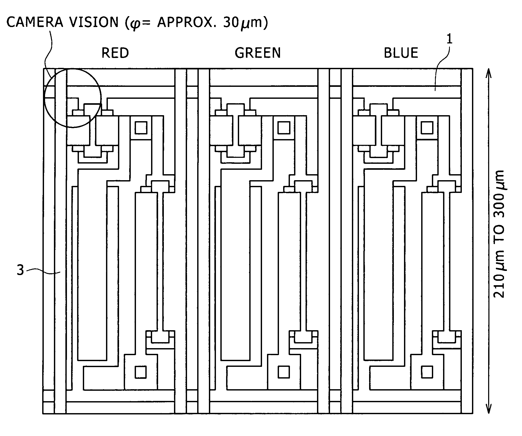
However, in this viewing field range, it takes a very long time to detect or repair many failing points in the display area.

Method used


Image

  • Display panel and panel inspection apparatus
  • Display panel and panel inspection apparatus
  • Display panel and panel inspection apparatus

Examples


embodiment 1

(C-1) Embodiment 1

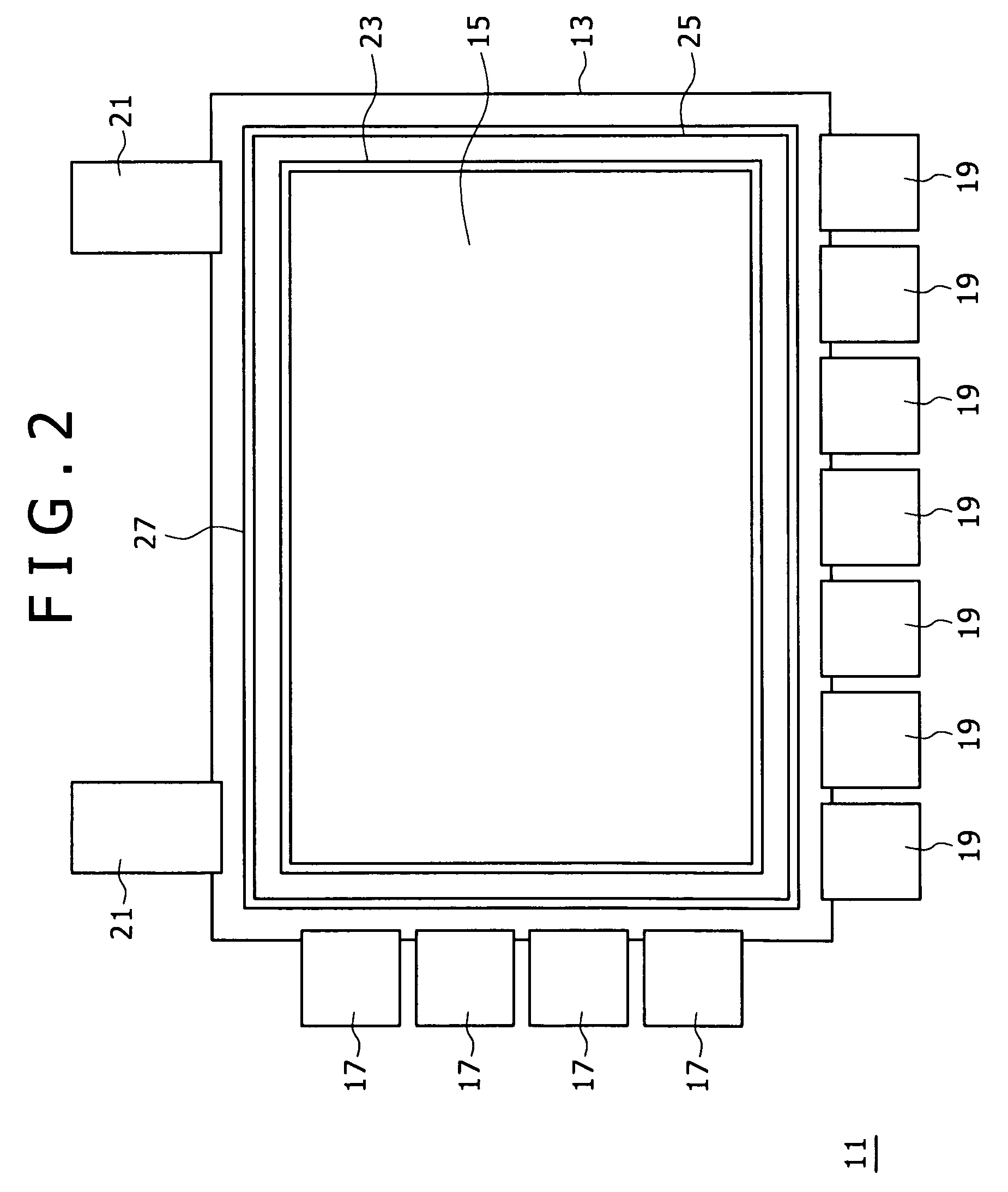
[0060]Referring to FIG. 10, there is shown an exemplary inspection apparatus configured to inspect an organic EL panel 41 with the above-mentioned positional identification pattern formed inside the display area. It should be noted that FIG. 10 shows a panel inspection apparatus having capabilities of detecting the positional coordinates of failing pixels.

[0061]Therefore, FIG. 10 shows merely a functional block configuration associated with the capabilities of detecting the positional coordinates of every detected failing pixel. The panel inspection apparatus shown in FIG. 10 has an imaging camera 43, a move block 45, a pattern comparison block 47, and a positional identification block 49.

[0062]It should be noted that the imaging camera 43 is an imaging device that has a magnifying capability equivalent to a microscope. The move block 45 is a movable device that relatively moves the organic EL panel 41 and the imaging camera 43.

[0063]The move block 45 is configured...

embodiment 2

(C-2) Embodiment 2

[0075]Referring to FIG. 12, there is shown an exemplary inspection apparatus for inspecting an organic EL panel 51 with the above-mentioned positional identification pattern formed inside the display area. It should be noted that FIG. 12 shows a panel inspection apparatus having a capability of aligning a repair area with a previously given failing point.

[0076]Therefore, FIG. 12 shows merely a functional block configuration associated with the moving function of the repair area. The panel inspection apparatus shown in FIG. 12 has an imaging camera 53, a pattern comparison block 55, a positional identification block 57, and a move block 59.

[0077]It should be noted that the imaging camera 53 is an imaging device that has a magnifying capability equivalent to a microscope. The pattern comparison block 55 is a processing unit configured to execute comparison between imaging pattern and positional identification pattern.

[0078]The positional identification block 57 is a ...


PUM


Abstract

Disclosed herein is a display panel based on active matrix driving having a display area made up of N pixel control lines, M video signal lines orthogonally intersecting the N pixel control lines, and pixel circuits arranged at intersections between the N pixel control lines and M video signal lines, wherein positional identification patterns are arranged on every k (k being a natural number) pixel control lines inside each of the pixel circuits.

Description

CROSS REFERENCES TO RELATED APPLICATIONS[0001]The present invention contains subject matter related to Japanese Patent Application JP 2007-237270 filed in the Japan Patent Office on Sep. 12, 2007, the entire contents of which being incorporated herein by reference.BACKGROUND OF THE INVENTION[0002]1. Field of the Invention[0003]The present invention relates to a technology configured to identify the pixel position of a display panel of active matrix drive type in a short time. It should be noted that the present invention has a mode as both a display panel and a panel inspection apparatus.[0004]2. Description of the Related Art[0005]Recently, various types of display technologies have been proposed as FPDs (Flat Panel Displays). For example, these display technologies include non-self-illuminating display technologies, such as LCD (Liquid Crystal Display), that use backlighting and self-illuminating display technologies, such as plasma display and organic EL (Electro Luminescence) di...

Claims


Application Information

Patent Timeline
Patent Type & Authority Patents(United States)
IPC IPC(8): H01L51/52
CPCG02F1/1309G09G3/12H04N17/04G09G3/006H10K59/131
Inventor NAKAMURA, KAZUO
Owner SONY GRP CORP
Learn More