Unlock instant, AI-driven research and patent intelligence for your innovation.

Method for operating semiconductor memory device

a memory device and semiconductor technology, applied in the field of semiconductor memory devices, can solve the problems of reducing the efficiency of data management in flash memory devices

Active Publication Date: 2013-08-20
SK HYNIX INC
View PDF4 Cites 3 Cited by
  • Summary
  • Abstract
  • Description
  • Claims
  • Application Information

AI Technical Summary

Benefits of technology

Enhances data management efficiency by allowing selective erasure and programming of memory blocks, enabling the same read data value for both first and second erased states, thus improving data handling and storage capabilities.

Problems solved by technology

However, even when only the selected pages should be erased, a flash memory device designed to erase data on a memory block-by-memory block basis may operate to erase the entire memory block, including the selected pages and unselected pages.
As a result, the efficiency of data management in the flash memory device is reduced.

Method used


Image

  • Method for operating semiconductor memory device
  • Method for operating semiconductor memory device
  • Method for operating semiconductor memory device

Examples


Embodiment Construction

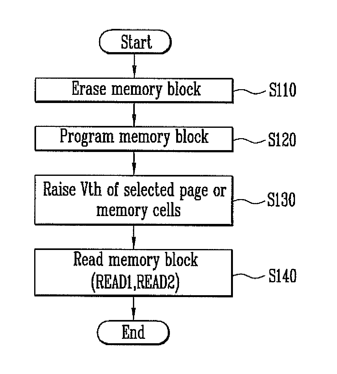
[0024]Hereinafter, various exemplary embodiments will be described more fully with reference to the accompanying drawings in which some exemplary embodiments are shown. However, specific structural and functional details disclosed herein are merely representative for purposes of describing exemplary embodiments of the present invention.

[0025]The terminology used herein is for the purpose of describing particular embodiments only and is not intended to limit all exemplary embodiments. As used herein, the singular forms “a,”“an” and “the” are intended to include the plural forms as well, unless the context clearly indicates otherwise. It will be further understood that the terms “comprises,”“comprising,”“includes” and / or “including,” when used herein, specify the presence of stated features, integers, steps, operations, elements, and / or components, but do not preclude the presence or addition of one or more other features, integers, steps, operations, elements, components, and / or grou...


PUM


Abstract

A method for operating a semiconductor memory device includes the steps of: erasing memory cells of a memory block to set the memory cells in a first erased state, programming a part of the memory cells of the memory block to convert them into a programmed state, raising threshold voltages of selected memory cells of the memory block and converting the selected memory cells from the programmed state to a second erased state, and reading data from the memory cells in the first erased state, the programmed state, and the second erased state, and outputting the data read from the memory cells in the first and second erased states with the same value.

Description

CROSS-REFERENCE TO RELATED APPLICATIONS[0001]The present application claims priority under 35 U.S.C 119(a) to Korean Application No. 10-2010-0066490, filed on Jul. 9, 2010, in the Korean Intellectual Property Office, which is incorporated by reference in its entirety.BACKGROUND[0002]1. Technical Field[0003]Embodiments of the present invention relate generally to semiconductor memory devices.[0004]2. Related Art[0005]A flash memory device is a type of semiconductor memory and is organized by including a plurality of memory cell blocks. Each memory cell block (or memory block) is normally composed of a plurality of cell strings in which a plurality of memory cells are coupled in series, a plurality of bit lines, a plurality of word lines, drain selection transistors coupled between the cell strings and bit lines, and source selection transistors coupled between the cell strings and a common source line. A group of memory cells sharing a word line may constitute a page. Memory cells in...

Claims


Application Information

Patent Timeline
Patent Type & Authority Patents(United States)
IPC IPC(8): G11C16/04
CPCG11C11/5628G11C11/5635G11C16/0483G11C16/10
Inventor JEONG, BYOUNG KWAN
Owner SK HYNIX INC