Semiconductor structure and fabrication method thereof

a semiconductor and semiconductor technology, applied in the field of semiconductor structure, can solve the problems of reducing the resistance of buried digit lines in memory arrays, and achieve the effect of improving the semiconductor structure of memory devices

Active Publication Date: 2013-09-17
NAN YA TECH
View PDF2 Cites 4 Cited by
  • Summary
  • Abstract
  • Description
  • Claims
  • Application Information

AI Technical Summary

Benefits of technology

[0007]It is one object of the present invention to provide an improved semiconductor structure for memory devices utilizing buried digit line architecture in order to solve the above-described prior art problems or shortcomings.

Problems solved by technology

However, as the packing density in integrated circuits increases, it becomes more difficult to reduce the resistance of a buried digit line in the memory array.

Method used


Image

  • Semiconductor structure and fabrication method thereof
  • Semiconductor structure and fabrication method thereof
  • Semiconductor structure and fabrication method thereof

Examples


Embodiment Construction

[0013]Reference will now be made in detail to example embodiments, examples of which are illustrated in the accompanying drawings. However, example embodiments are not limited to the embodiments illustrated hereinafter, and the embodiments herein are rather introduced to provide easy and complete understanding of the scope and spirit of the invention. In the drawings, the thicknesses of layers and regions may be exaggerated for clarity.

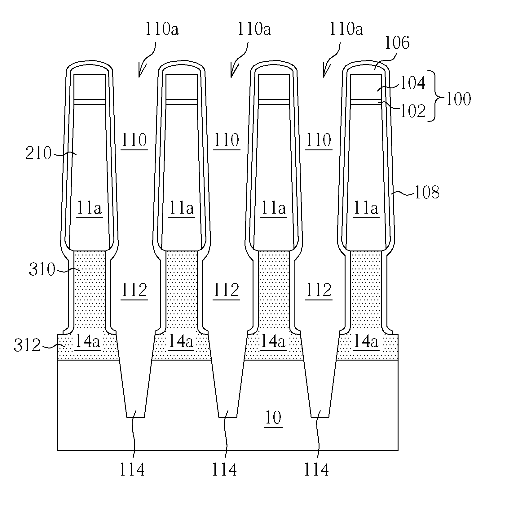
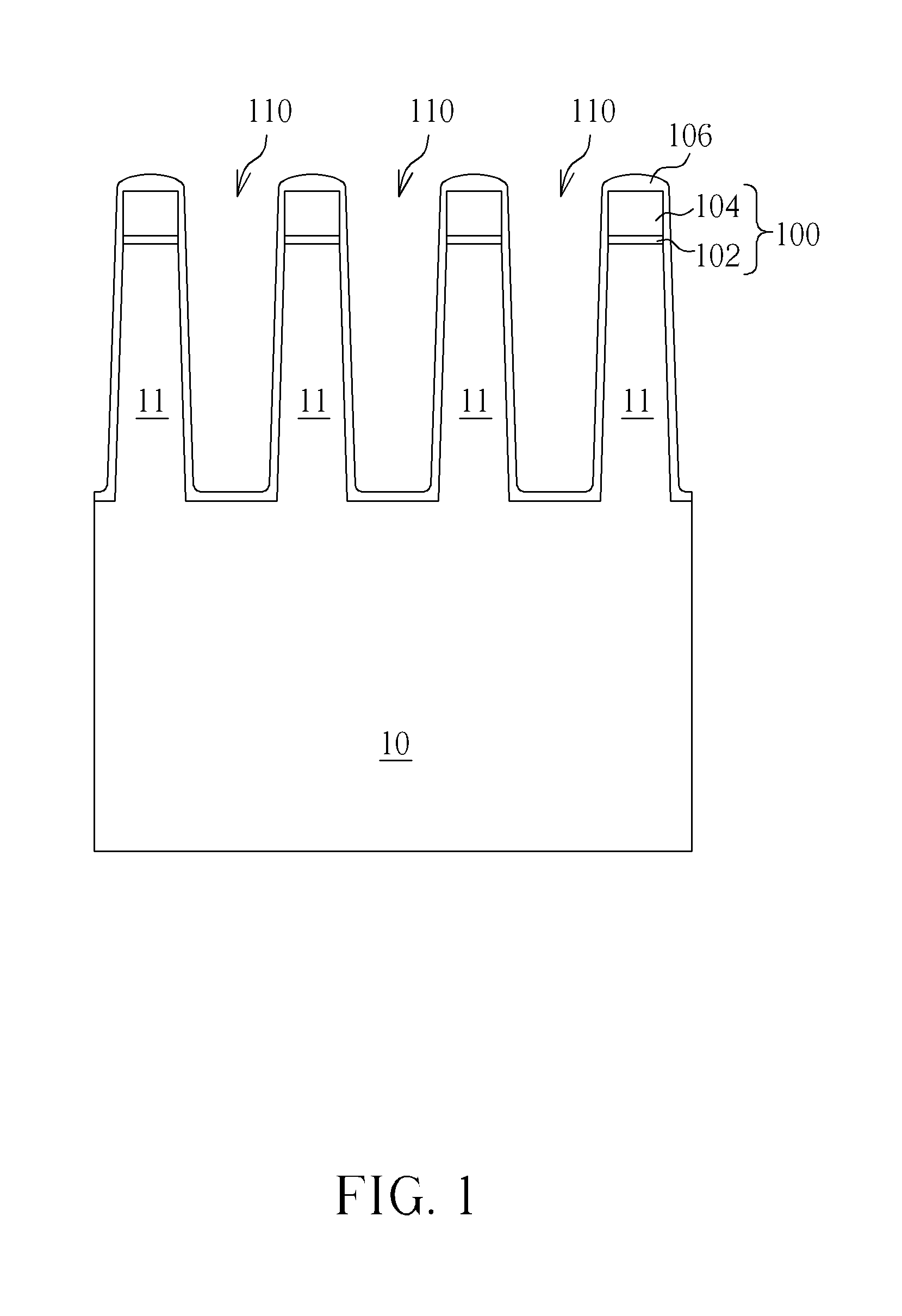
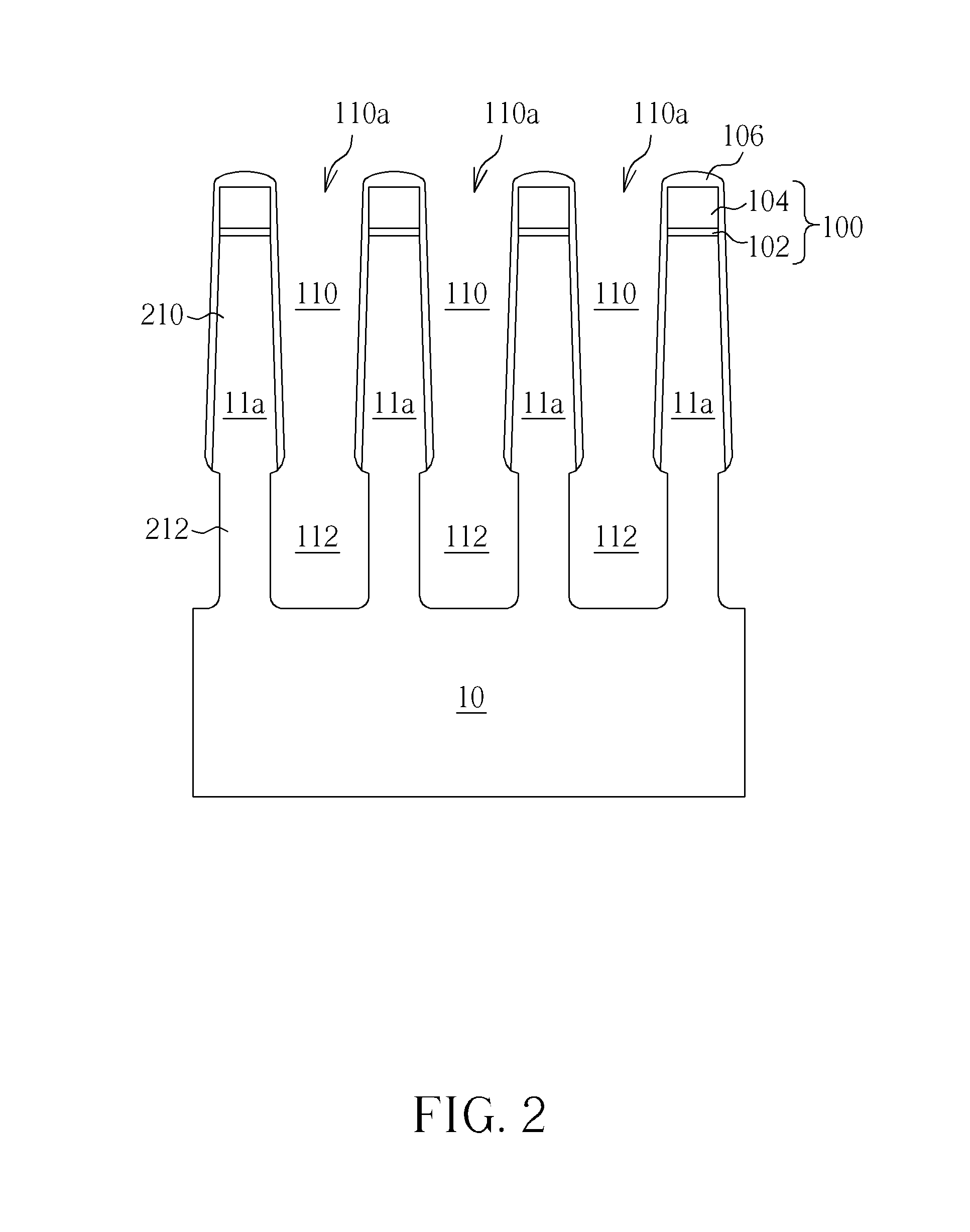
[0014]Referring to FIG. 1 to FIG. 5, a method for fabricating a memory structure having a low-resistance buried digit line is illustrated according to one embodiment of this invention. As shown in FIG. 1, a semiconductor substrate 10 such as a silicon substrate is provided. A patterned hard mask 100 may be provided on a major surface of the semiconductor substrate 10. According to the embodiment, the patterned hard mask 100 may comprise a silicon oxide layer 102 and a silicon nitride layer 104. It is understood that the patterned hard mask 100 may com...


PUM


Abstract

A semiconductor structure includes a semiconductor substrate having thereon a plurality of deep trenches and a plurality of pillar structures between the deep trenches, wherein each of the plurality of pillar structures comprises an upper portion and a lower portion. A doping region is formed in the lower portion. A diffusion barrier layer is disposed on a sidewall of the lower portion.

Description

BACKGROUND OF THE INVENTION[0001]1. Field of the Invention[0002]The present invention relates generally to a semiconductor structure and, more particularly, to an improved memory structure having low-resistance buried digit lines and method of forming the same.[0003]2. Description of the Prior Art[0004]Electronic storage devices such as dynamic random access memory (DRAM) have been an essential resource for the retention of data. Conventional semiconductor DRAM typically incorporate capacitor and transistor structures in which the capacitors temporarily store data based on the charged state of the capacitor structure. In general, this type of semiconductor memory often requires densely packed capacitor structures that are easily accessible for electrical interconnection.[0005]The capacitor and transistor structures are generally known as memory cells. The memory cells are arranged into memory arrays. The memory cells are addressed via a word line and a digit line, one of which addre...

Claims


Application Information

Patent Timeline
Patent Type & Authority Patents(United States)
IPC IPC(8): H01L29/94
CPCH01L27/10885H10B12/482
Inventor YU, CHIEN-ANCHANG, YUAN-SUNGCHEN, FENG-LINGCHIEN, CHUN-HUNG
Owner NAN YA TECH
Why Eureka
Try Eureka