PIN diode structure with zinc diffusion region

a diode and zinc diffusion technology, applied in the field of pin photodiodes, can solve the problems of high recombination current, high recombination current, and often degraded dielectric protection

Inactive Publication Date: 2009-05-26
EMCORE INC
View PDF1 Cites 3 Cited by
  • Summary
  • Abstract
  • Description
  • Claims
  • Application Information

AI Technical Summary

Benefits of technology

[0010]It is an object of the present invention to provide an improved semiconductor structure for a PIN photodiode with a zinc diffusion region.
[0013]It is also an object of the present invention to provide a process to provide a protected PIN junction in a PIN photodiode and thereby provide consistent fabrication and reliability of such devices.
[0021]The protection of the PN junction in the PIN diode as a result of the fabrication process of the present invention is a substantial improvement of the PN diode reliability and lifetime, particularly under extreme conditions such as those conditions simulated under testing at 85 degrees Centigrade and 85% humidity conditions.

Problems solved by technology

However, the dielectric protection often degrades under various reliability test environments such as high temperature, high humidity test (HTHH), etc.
One of the drawbacks for the traditional process is that there is an exposed PN junction on the surface of the top InGaAs or InP layer.
Without re-depositing a dielectric layer for high quality passivation, the surface recombination current is potentially high, which gives rise to inconsistent operating dark current after fabrication.
Even with good initial leakage characteristics, significant degradation of operation dark current often exists after aging, especially under conditions of high temperatures operating live (HTOL) tests of high temperature / high humidity reverse biased tests (THRB), where dielectric protection is normally weak if attacked by corrosion.

Method used


Image

  • PIN diode structure with zinc diffusion region
  • PIN diode structure with zinc diffusion region
  • PIN diode structure with zinc diffusion region

Examples


Embodiment Construction

[0045]Details of the present invention will now be described, including exemplary aspects and embodiments thereof. Referring to the drawings and the following description, like reference numbers are used to identify like or functionally similar elements, and are intended to illustrate major features of the exemplary embodiments in a highly simplified diagrammatic manner. Moreover, the drawings are not intended to depict every feature of actual embodiments nor the relative dimension of the depicted elements, and are not drawn to scale.

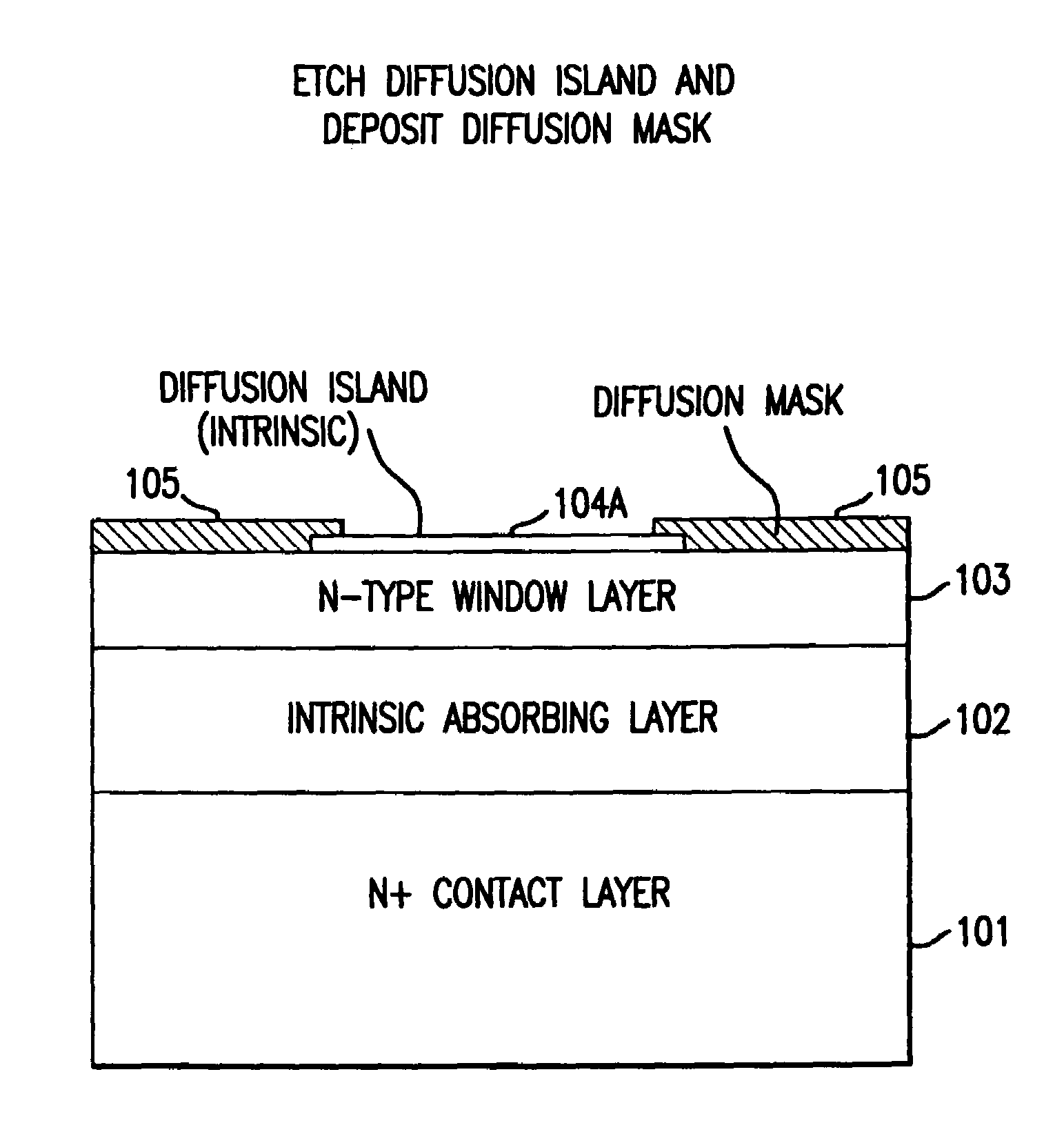
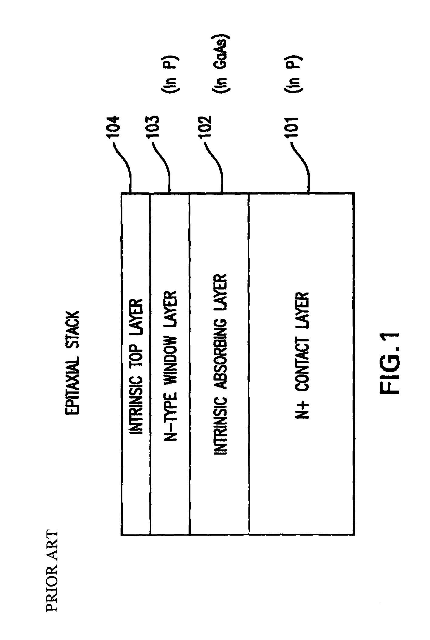
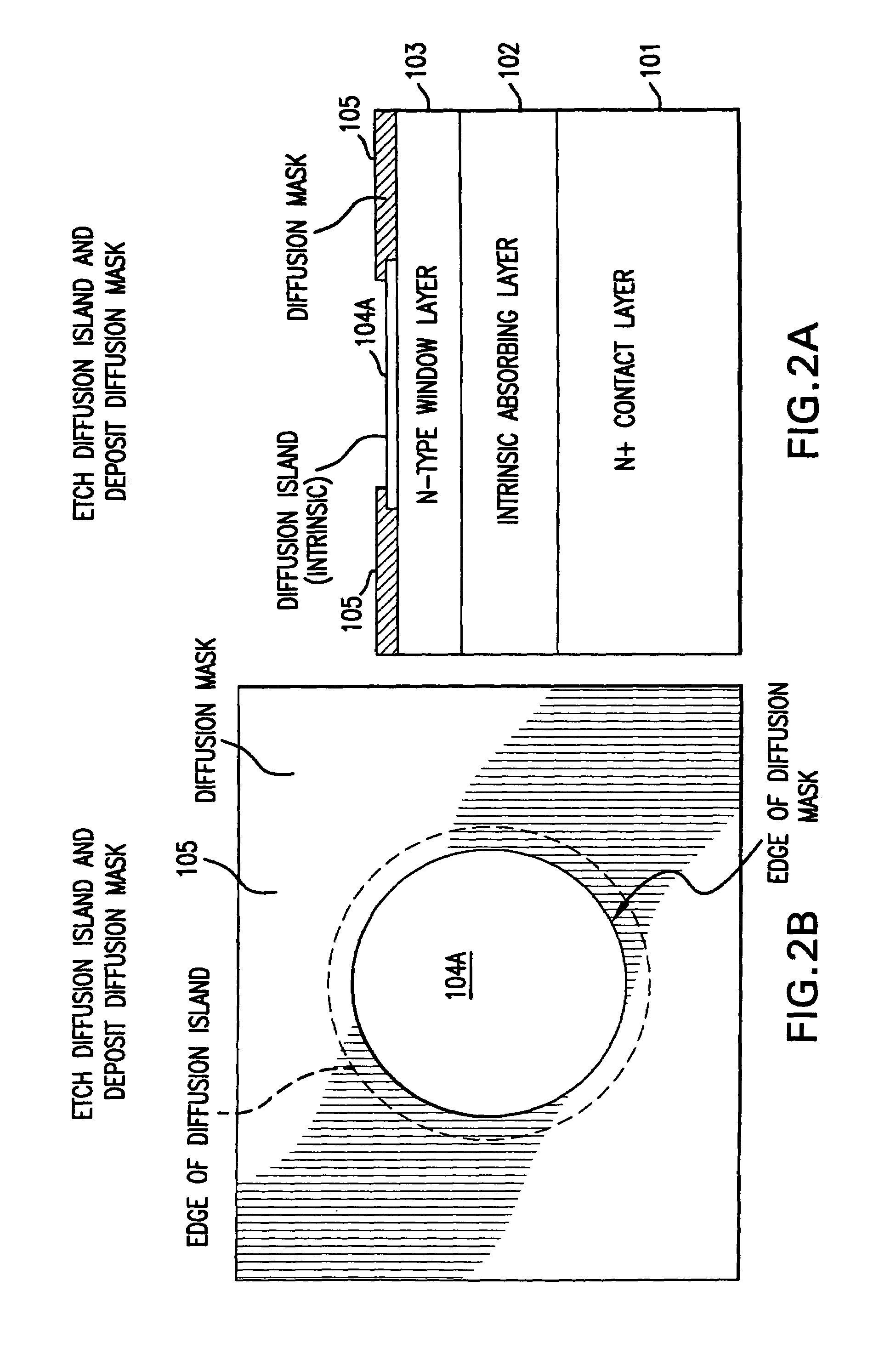
[0046]Referring to FIG. 1, there is shown a fragmentary, cross-sectional view of a semi-conductor structure or the epitaxial stack representing the initial layers of a lateral PIN photodiode during the fabrication process of the present invention that is depicted with generic first and second type electrodes. In particular, the photodiode 100 includes an n+ contact layer 101 and an intrinsic absorbing layer 102 disposed on the n+ contact layer. An n-typ...


PUM


Abstract

A PIN photodiode having a substrate, a first type electrode layer disposed on the substrate, a first layer of intrinsic material disposed over a portion of the first-type electrode layer, a first type window layer disposed over said intrinsic layer. An island shaped region of intrinsic material is disposed over the window layer and a dielectric layer disposed over the island region and at least the peripheral portion of said island shaped region whereby an opening is formed in the island shaped region. A dopant is diffused through the opening so as to form a PN junction that extends into the first layer of intrinsic material.

Description

CROSS REFERENCE TO RELATED APPLICATION[0001]This application claims priority to and the benefit of U.S. Provisional Application No. 60 / 611,152 filed Sep. 20, 2004.BACKGROUND OF THE INVENTION[0002]1. Field of the Invention[0003]The invention relates generally to PIN photodiodes. More particularly, the invention relates to a PIN photodiode semiconductor structure diode which has high reliability, with extremely low dark current, and suitable to be used in high temperature, high humidity environments, and processes for fabrication of such devices.[0004]2. Description of the Related Art[0005]Fiber optic communications typically employ a modulated light source, such as a laser, a photodiode light detector, and an optical fiber interconnecting the laser and the photodiode. The laser is modulated to emit light pulses that are transmitted over an optical fiber and received at a remote unit that includes a photodiode to convert the optical signal into an electrical signal. In particular, PIN...

Claims


Application Information

Patent Timeline
Patent Type & Authority Patents(United States)
IPC IPC(8): H01L27/15
CPCH01L31/105
Inventor GAO, XIANGCERUZZI, ALEXLIU, LINLINSCHWED, STEPHEN
Owner EMCORE INC
Why Eureka
Try Eureka