

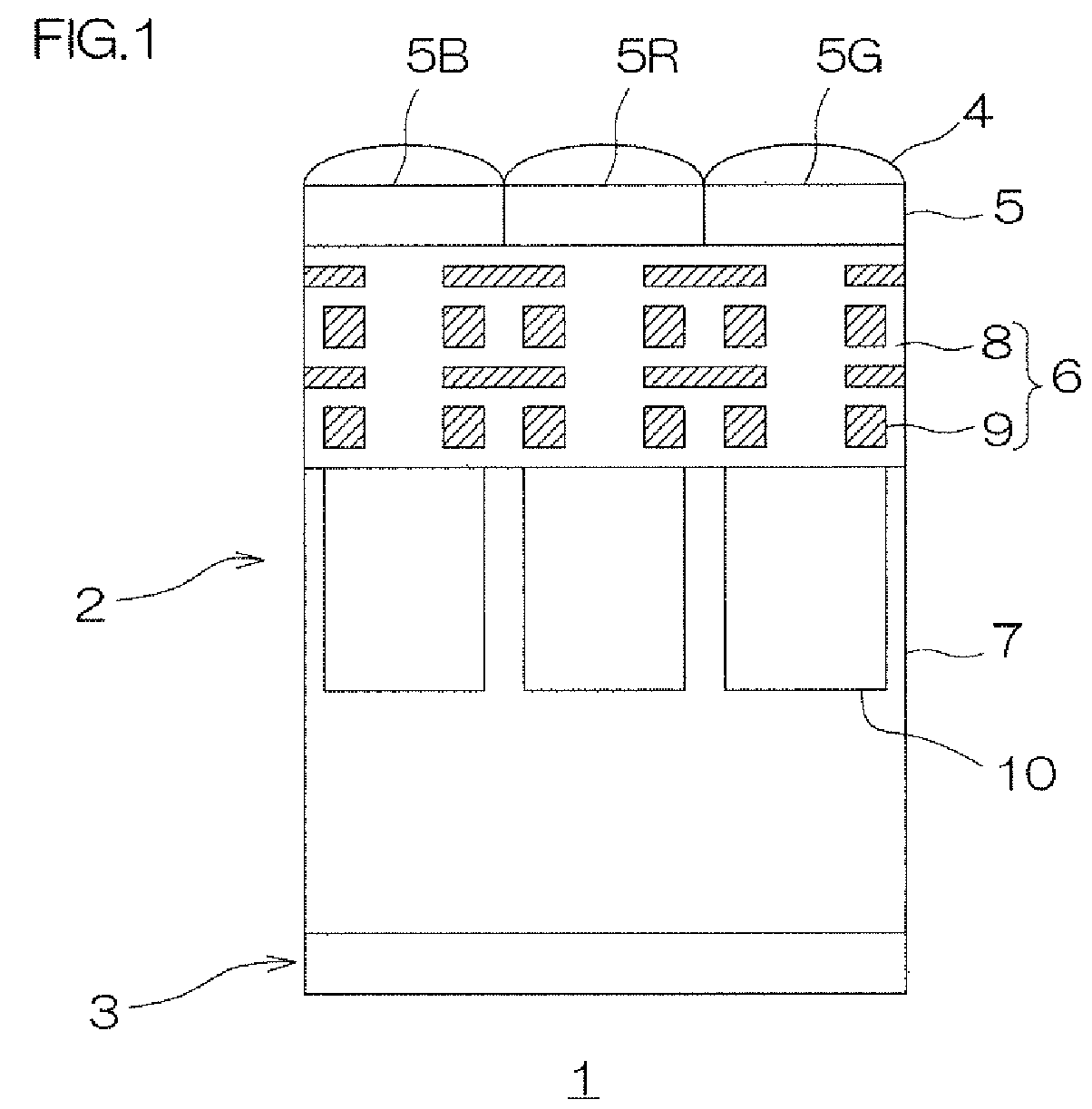
Imaging device module
a technology of imaging device and module, which is applied in the direction of color television, television system scanning details, television systems, etc., can solve the problems of cost disadvantage, and achieve the effect of excellent heat dissipation and cost reduction
- Summary
- Abstract
- Description
- Claims
- Application Information
AI Technical Summary
Benefits of technology
Problems solved by technology
Method used
Image

Examples
production example 1
Production of Thermal Conductive Sheet
[0204]The components described below were blended, stirred, and allowed to stand at room temperature (23° C.) for one night, thereby allowing methyl ethyl ketone (dispersion medium for the curing agent) to volatilize and preparing a semi-solid mixture. The details of the components were as follows: 13.42 g of PT-110 (trade name, plate-like boron nitride particles, average particle size (light scattering method) 45 μm, manufactured by Momentive Performance Materials Inc.), 1.0 g of jER®828 (trade name, bisphenol A epoxy resin, first epoxy resin, liquid, epoxy equivalent 184 to 194 g / eqiv., softening temperature (ring and ball method) below 25° C., melt viscosity (80° C.) 70 mPa·s, manufactured by Japan Epoxy Resins Co., Ltd.), 2.0 g of EPPN-501HY (trade name, triphenylmethane epoxy resin, second epoxy resin, solid, epoxy equivalent 163 to 175 g / eqiv., softening temperature (ring and ball method) 57 to 63° C., manufactured by NIPPON KAYAKU Co., Lt...
production examples 2 to 9 and 11 to 16
[0210]Thermal conductive sheets were obtained in the same manner as in Production Example 1, based on the mixing ratio and the production conditions of Tables 1 to 3.
production example 10
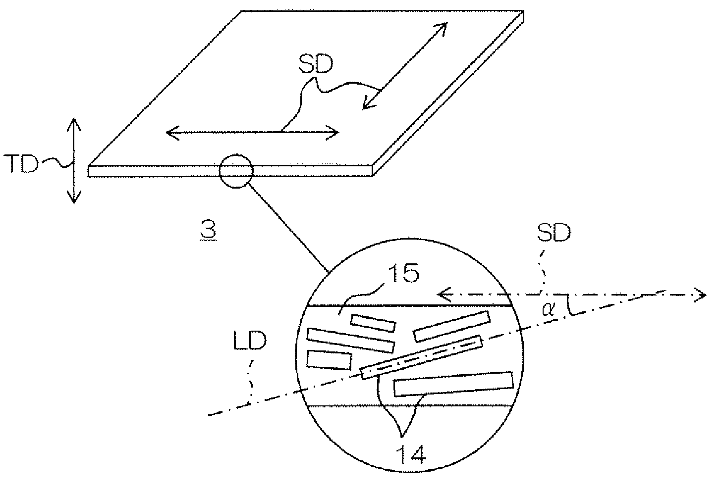
[0211]A mixture was prepared by blending and stirring components (boron nitride particles and polyethylene) in accordance with the mixing formulation of Table 2. That is, during the stirring of the components, the mixture was heated to 130° C., and polyethylene was melted.
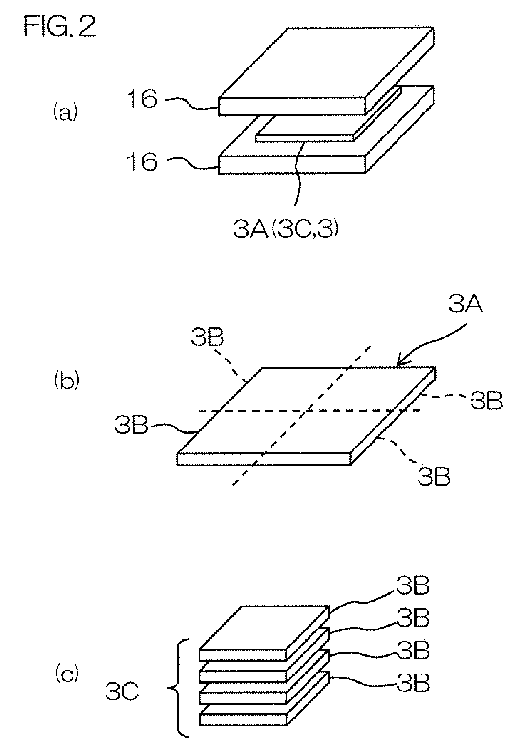
[0212]Then, the obtained mixture was sandwiched by two silicone-treated releasing films, and then these were hot-pressed with a vacuum hot-press at 120° C. under an atmosphere (vacuum atmosphere) of 10 Pa with a load of 1 ton (4 MPa) for 2 minutes. A pressed sheet having a thickness of 0.3 mm was thus obtained (ref: FIG. 2 (a)).
[0213]Thereafter, the obtained pressed sheet was cut so as to be divided into a plurality of pieces when projected in the thickness direction of the pressed sheet. Divided sheets were thus obtained (ref: FIG. 2 (b)). Next, the divided sheets were laminated in the thickness direction. A laminated sheet was thus obtained (ref: FIG. 2 (c)).
[0214]Then, the obtained laminated sheet was hot-presse...
PUM
 Abstract
Description
Claims
Application Information