Semiconductor pressure sensor

a technology of semiconductors and sensors, applied in the direction of fluid pressure measurement, fluid pressure measurement by electric/magnetic elements, instruments, etc., can solve the problems of difficult control of difficulty in adjusting the depth, and difficulty in adjusting the size and position of the diaphragm, so as to reduce the occurrence of measurement errors, reduce the relative positional deviation, and reduce the effect of measurement error

Active Publication Date: 2013-10-08
ALPS ALPINE CO LTD
View PDF14 Cites 0 Cited by
  • Summary
  • Abstract
  • Description
  • Claims
  • Application Information

AI Technical Summary

Benefits of technology

[0012]The present invention provides a semiconductor pressure sensor exhibiting a small relative positional deviation between a diaphragm and piezo-resistance elements or a small error in shape of a diaphragm so as to reduce occurrences of measurement error.
[0013]A semiconductor pressure sensor according to an aspect of the present invention includes a cavity disposed in one silicon substrate of a SOI substrate having two silicon substrates bonded to each other with an oxide film therebetween and a diaphragm formed from the other silicon substrate and the oxide film, wherein the oxide film, bordering the above-described cavity, of the diaphragm includes an arc-shaped section at the boundary portion to the above-described one silicon substrate defining the inner wall side surface of the cavity, the arc-shaped section having the same width as the width of the cavity at a desired section in the one silicon substrate and reducing the width of the cavity from the boundary portion toward the diaphragm center.
[0014]Preferably, the oxide film, bordering the above-described cavity, of the diaphragm is disposed in such a way as to have a thickness reducing from the above-described boundary portion toward the central portion of the diaphragm and have a region with a small thickness. According to this configuration, the sensitivity error of the diaphragm can be reduced.

Problems solved by technology

It is difficult to control the amount, the depth, and the like of the eroded portion 112a due to over etching and, therefore, it is difficult to control the size and the position of the diaphragm 121.
In this regard, deviation of the size of the diaphragm 121 from the design value causes an error likewise.

Method used


Image

  • Semiconductor pressure sensor
  • Semiconductor pressure sensor
  • Semiconductor pressure sensor

Examples


Embodiment Construction

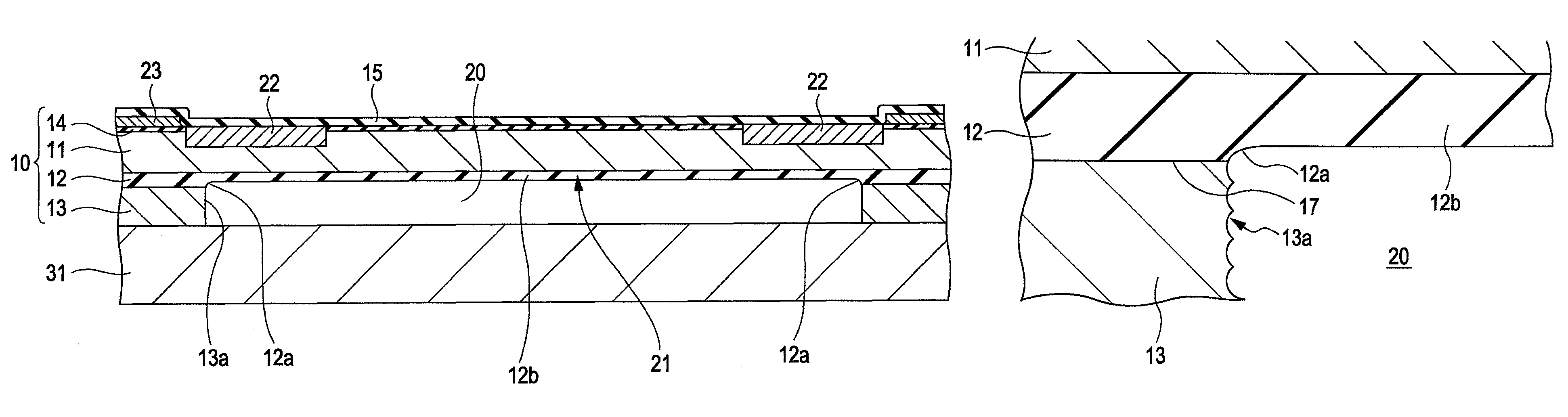
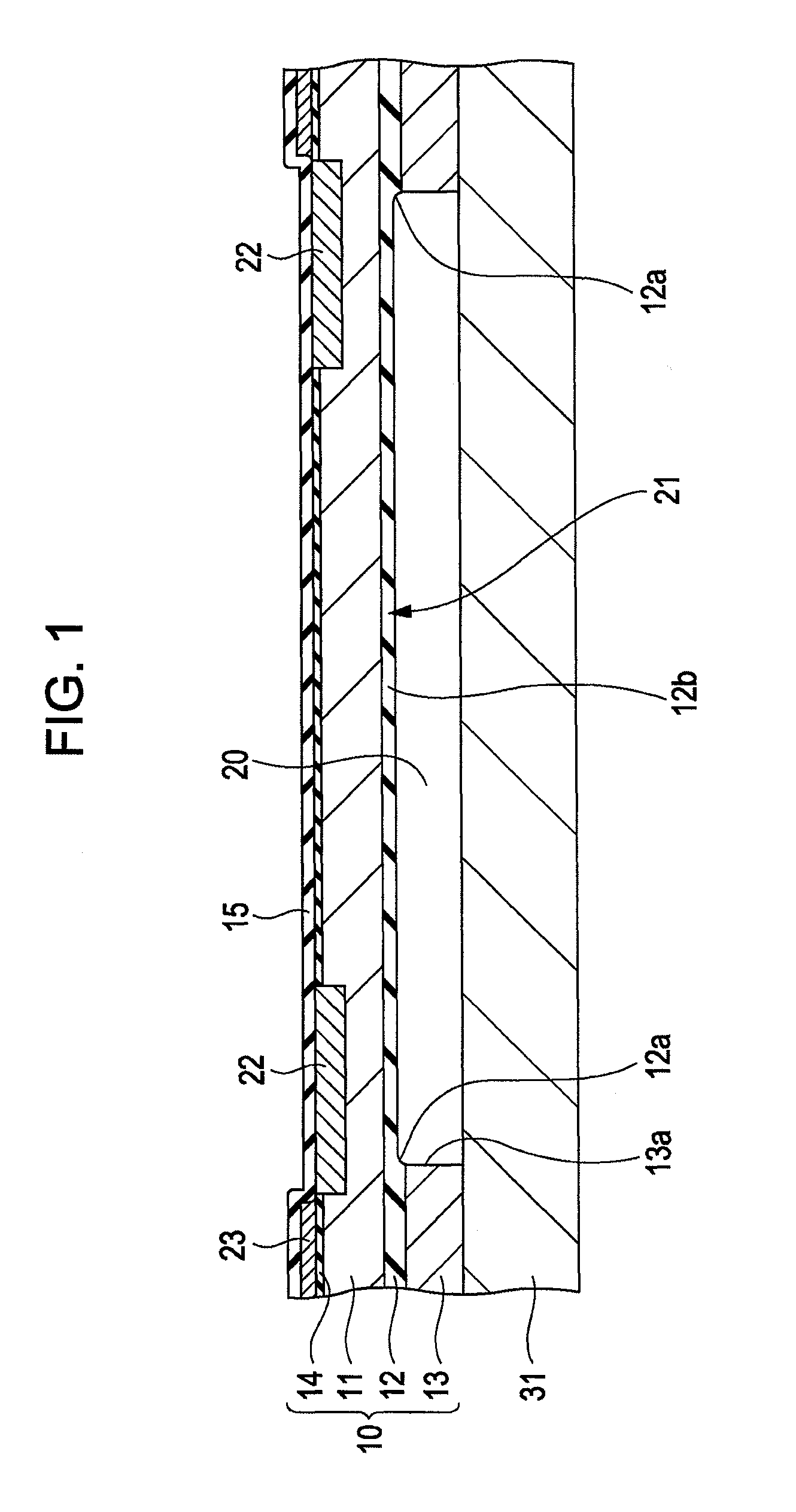
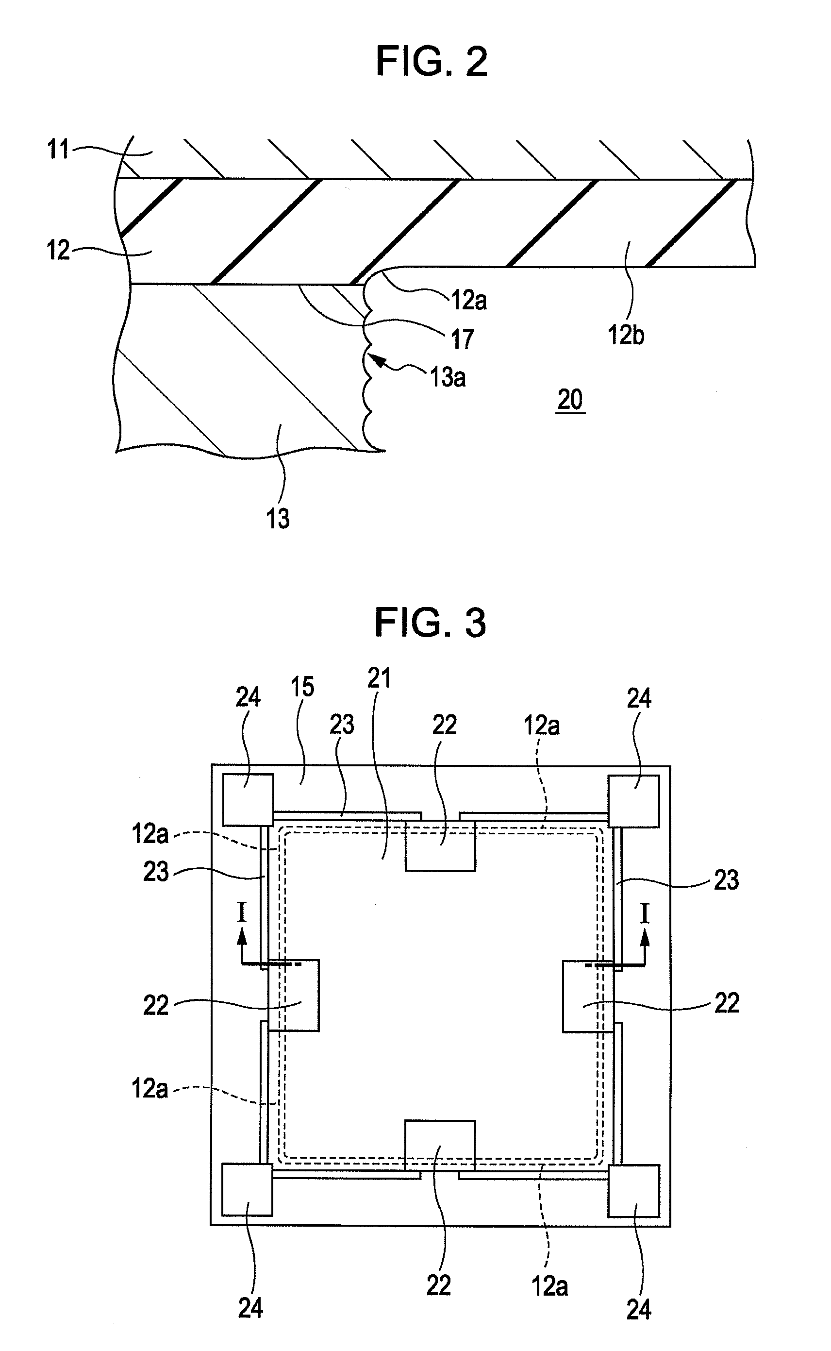
[0028]The preferred embodiments according to the present invention will be described with reference to the drawings. FIG. 1 is a sectional view showing the section of a key portion of a diaphragm type semiconductor pressure sensor according to an embodiment of the present invention, taken along a line I-I shown in FIG. 3. FIG. 2 is a magnified sectional view of a boundary portion between a silicon substrate defining the inner wall side surface of a cavity and a diaphragm oxide film bordering the cavity shown in FIG. 1. FIG. 3 is a plan view showing a key portion of the semiconductor pressure sensor.

[0029]Initially, a silicon on insulator (SOI) substrate 10 provided with piezo-resistance elements 22, wirings 23, and pads 24 is prepared. In this SOI substrate 10, a first silicon substrate 11 and a second silicon substrate 13 are bonded to each other with a silicon oxide (SiO2) film 12 serving as an oxide film therebetween. A silicon oxide film 14 serving as an oxide film is disposed o...


PUM


Abstract

A semiconductor pressure sensor includes a cavity disposed in one silicon substrate of a SOI substrate having two silicon substrates bonded to each other with an oxide film therebetween and a diaphragm formed from the other silicon substrate and the oxide film, wherein the oxide film, bordering the cavity, of the diaphragm includes an arc-shaped section at the boundary portion to the one silicon substrate defining the inner wall side surface of the cavity, the arc-shaped section having the same width as the width of the cavity at a desired section in the one silicon substrate and reducing the width of the cavity from the boundary portion toward the diaphragm center.

Description

RELATED APPLICATIONS[0001]This application is a Continuation of International Application No. PCT / JP2008 / 067239 filed on Sep. 25, 2008, which claims benefit of the Japanese Patent Application No. 2007-247085 filed on Sep. 25, 2007 and Japanese Patent Application No. 2008-007682 filed on Jan. 17, 2008, all of which are hereby incorporated by reference.BACKGROUND OF THE INVENTION[0002]1. Field of the Invention[0003]The present invention relates to semiconductor pressure sensor to measure pressures, e.g., air pressure.[0004]2. Description of the Related Art[0005]Previously, diaphragm type semiconductor pressure sensors have been known as semiconductor pressure sensors to measure automobile tire pressures and the like (refer to Japanese Unexamined Patent Application Publication Nos. 2001-358345, 2001-352078, 2002-208708, 5-063211, 2002-071493, and 2002-350259).[0006]FIG. 6 shows a cross-sectional structure of a semiconductor pressure sensor in a related art. This semiconductor pressure ...

Claims


Application Information

Patent Timeline
Patent Type & Authority Patents(United States)
IPC IPC(8): H01L29/84
CPCG01L9/0042G01L9/0054H01L29/84
Inventor ADACHI, TAKUYAKIKUIRI, KATSUYAFUKUDA, TETSUYAOKAWA, HISANOBUMINAGAWA, TAKAYUKI
Owner ALPS ALPINE CO LTD
Why Eureka
Try Eureka