
Lens heating compensation systems and methods

a technology of heating compensation and lens, applied in the field of lens heating compensation systems and methods, can solve the problems of difficult to reproduce a pattern on the wafer, large cost of making high-end mask sets, and general inability to apply opc, etc., and achieve high speed, high capacity, and high accuracy.

Active Publication Date: 2013-10-29
ASML NETHERLANDS BV
View PDF18 Cites 18 Cited by
  • Summary
  • Abstract
  • Description
  • Claims
  • Application Information

AI Technical Summary

Benefits of technology

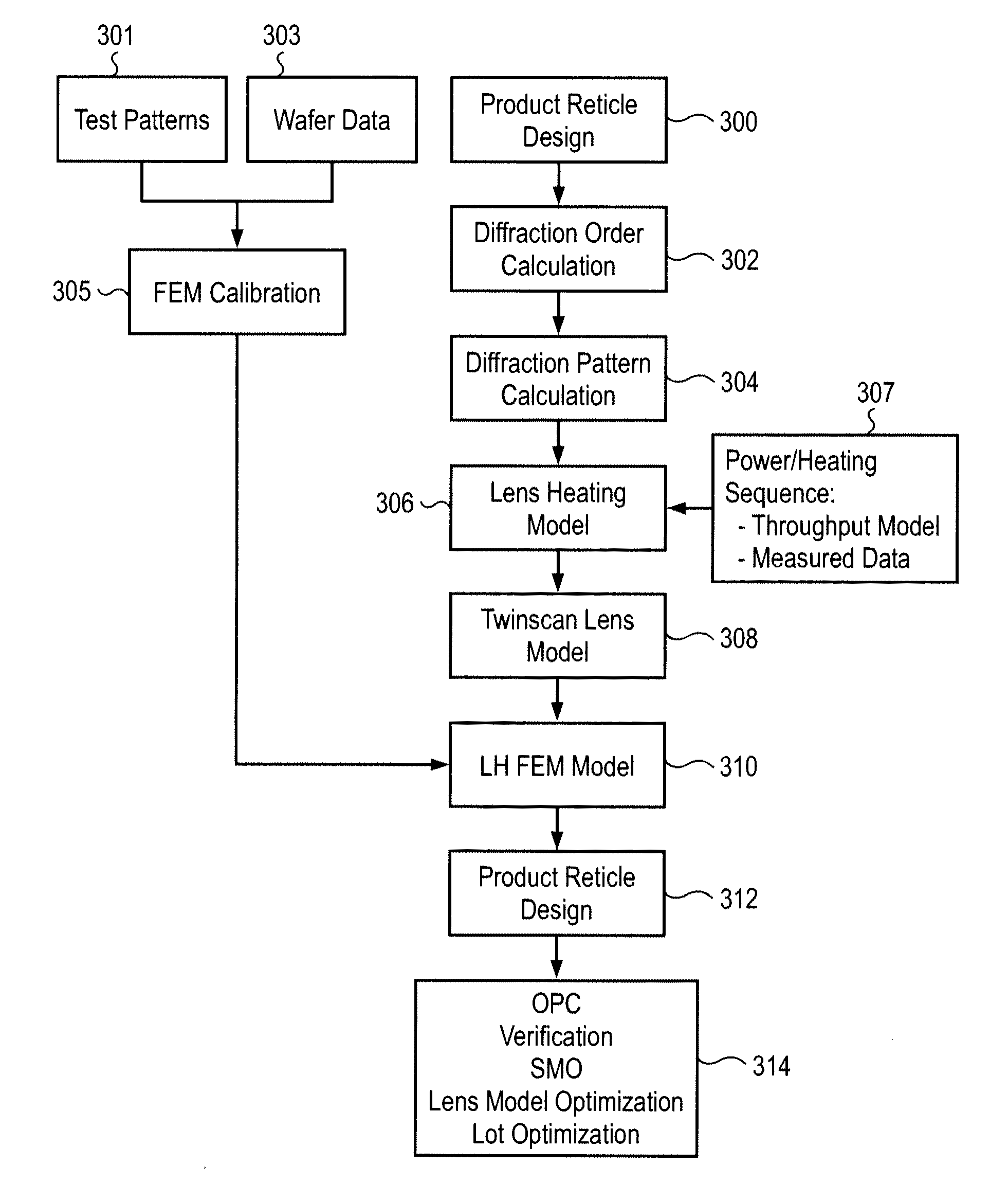
[0022]Certain embodiments of the invention provide optimization and correction systems and methods for photolithography systems. Methods include processes for optimizing lens manipulators in order to minimize impact of lens heating on lithographical metrics, particularly where the impact is characterized by a nonlinear relationship to aberration. These methods accommodate nonlinear metrics and can avoid issues associated with from the use of methods that handle nonlinear effects indirectly. Certain embodiments can be employed in systems that involve nonlinear litho metrics, including lens heating models and simulations, applications of lens heating simulations and application specific lens heating control using an image tuner. In some embodiments, the typically non-linear effects of lens heating on CDs may require litho metrics to be a linear function of Zernike polynomials.
[0026]Certain embodiments incorporate lens heating modeling full-chip lithography simulation systems. Full-chip verification can be applied to identify lens heating induced hot spots and verify lens heating corrections and lens heating aware OPC can be used to mitigate the lens heating impact on image quality.

Problems solved by technology

These rules are set by processing and design limitations.
In general, the smaller k1, the more difficult it becomes to reproduce a pattern on the wafer that resembles the shape and dimensions planned by a circuit designer in order to achieve particular electrical functionality and performance.
However, applying OPC is generally not an ‘exact science’, but an empirical, iterative process that does not always resolve all possible weaknesses on a layout.
This is driven by the enormous cost of making high-end mask sets, which run in the multi-million dollar range, as well as by the impact on turn-around time by reworking or repairing actual masks once they have been manufactured.
While full-chip numerical simulation of the lithographic patterning process has been demonstrated at a single process condition, typically best focus and best exposure dose or best ‘nominal’ condition, it is well known that manufacturability of a design requires sufficient tolerance of pattern fidelity against small variations in process conditions that are unavoidable during actual manufacturing.
However, such an increase in the computational time is prohibitive when attempting to validate and / or design a given target circuit.
However, such an assumption that the source distribution is uniform in each source region is not always valid, and as a result the effectiveness of this approach suffers.
Though these methods have demonstrated some successes, they typically require multiple complicated iterations to converge.
In addition, it may be difficult to determine the appropriate / optimal values for some extra parameters, such as γ in Granik's method, which dictates the trade-off between optimizing the source for wafer image fidelity and the smoothness requirement of the source.
Lens heating can adversely affect the operation of photolithographic systems by causing non uniform expansion and distortions of the lens which can cause variations in nominal numerical aperture value.
Lens heating can induce aberrations that can cause printing defects on wafers.
The effects of lens heating on CDs are typically non-linear and, generally, conventional systems cannot use linear mathematical models as a consequence.

Method used


Image

  • Lens heating compensation systems and methods
  • Lens heating compensation systems and methods
  • Lens heating compensation systems and methods

Examples


Embodiment Construction

[0043]Embodiments of the present invention will now be described in detail with reference to the drawings, which are provided as illustrative examples so as to enable those skilled in the art to practice the invention. Notably, the figures and examples below are not meant to limit the scope of the present invention to a single embodiment, but other embodiments are possible by way of interchange of some or all of the described or illustrated elements. Wherever convenient, the same reference numbers will be used throughout the drawings to refer to same or like parts. Where certain elements of these embodiments can be partially or fully implemented using known components, only those portions of such known components that are necessary for an understanding of the present invention will be described, and detailed descriptions of other portions of such known components will be omitted so as not to obscure the invention. In the present specification, an embodiment showing a singular compon...


PUM


Abstract

Methods for calibrating a photolithographic system are disclosed. A cold lens contour for a reticle design and at least one hot lens contour for the reticle design are generated from which a process window is defined. Aberrations induced by a lens manipulator are characterized in a manipulator model and the process window is optimized using the manipulator model. Aberrations are characterized by identifying variations in critical dimensions caused by lens manipulation for a plurality of manipulator settings and by modeling behavior of the manipulator as a relationship between manipulator settings and aberrations. The process window may be optimized by minimizing a cost function for a set of critical locations.

Description

CROSS REFERENCE TO RELATED APPLICATIONS[0001]The present application claims priority to U.S. Provisional Patent Appln. No. 61 / 058,502 filed Jun. 3, 2008 and to U.S. Provisional Patent Appln. No. 61 / 122,537 filed Dec. 15, 2008, the contents of which are incorporated herein by reference in their entirety.BACKGROUND OF THE INVENTION[0002]1. Field of the Invention[0003]The present invention relates generally to systems and methods for performing model-based scanner tuning and optimization and more particularly to optimization of performance of multiple lithography systems.[0004]2. Description of Related Art[0005]Lithographic apparatus can be used, for example, in the manufacture of integrated circuits (ICs). In such a case, the mask may contain a circuit pattern corresponding to an individual layer of the IC, and this pattern can be imaged onto a target portion (e.g. comprising one or more dies) on a substrate (silicon wafer) that has been coated with a layer of radiation-sensitive mate...

Claims


Application Information

Patent Timeline
Patent Type & Authority Patents(United States)
IPC IPC(8): G03B27/52
CPCG03F7/70266G03F7/705G03F7/706G03F7/70891G06F17/50G03F7/70441G06F30/00G03F7/70504
Inventor YE, JUNLIU, PENGCAO, YU
Owner ASML NETHERLANDS BV
Learn More