Organic EL panel and method of manufacturing the same

a technology el panels, which is applied in the direction of organic semiconductor devices, thermoelectric devices, solid-state devices, etc., can solve the problems of high probability of defect generation in which portions of interconnects (e.g., pixel electrodes) on the surface of tft panels are lost, and achieve rapid and inexpensive manufacturing of organic el panels, short time, and lessen luminance reduction

Active Publication Date: 2013-11-19
JOLED INC
View PDF25 Cites 0 Cited by
  • Summary
  • Abstract
  • Description
  • Claims
  • Application Information

AI Technical Summary

Benefits of technology

[0042]The present invention enables to lessen luminance reductions at defects in pixel electrodes in short time without relying on expensive equipment. The present invention thus enables rapid and inexpensive manufacture of organic EL panels having minimized luminance unevenness.

Problems solved by technology

Recent increases in size and definition of organic EL panels has resulted in high probability of generation of defects in which portions of interconnects (e.g., pixel electrodes) on the TFT panel's surface are lost.

Method used


Image

  • Organic EL panel and method of manufacturing the same
  • Organic EL panel and method of manufacturing the same
  • Organic EL panel and method of manufacturing the same

Examples


Embodiment Construction

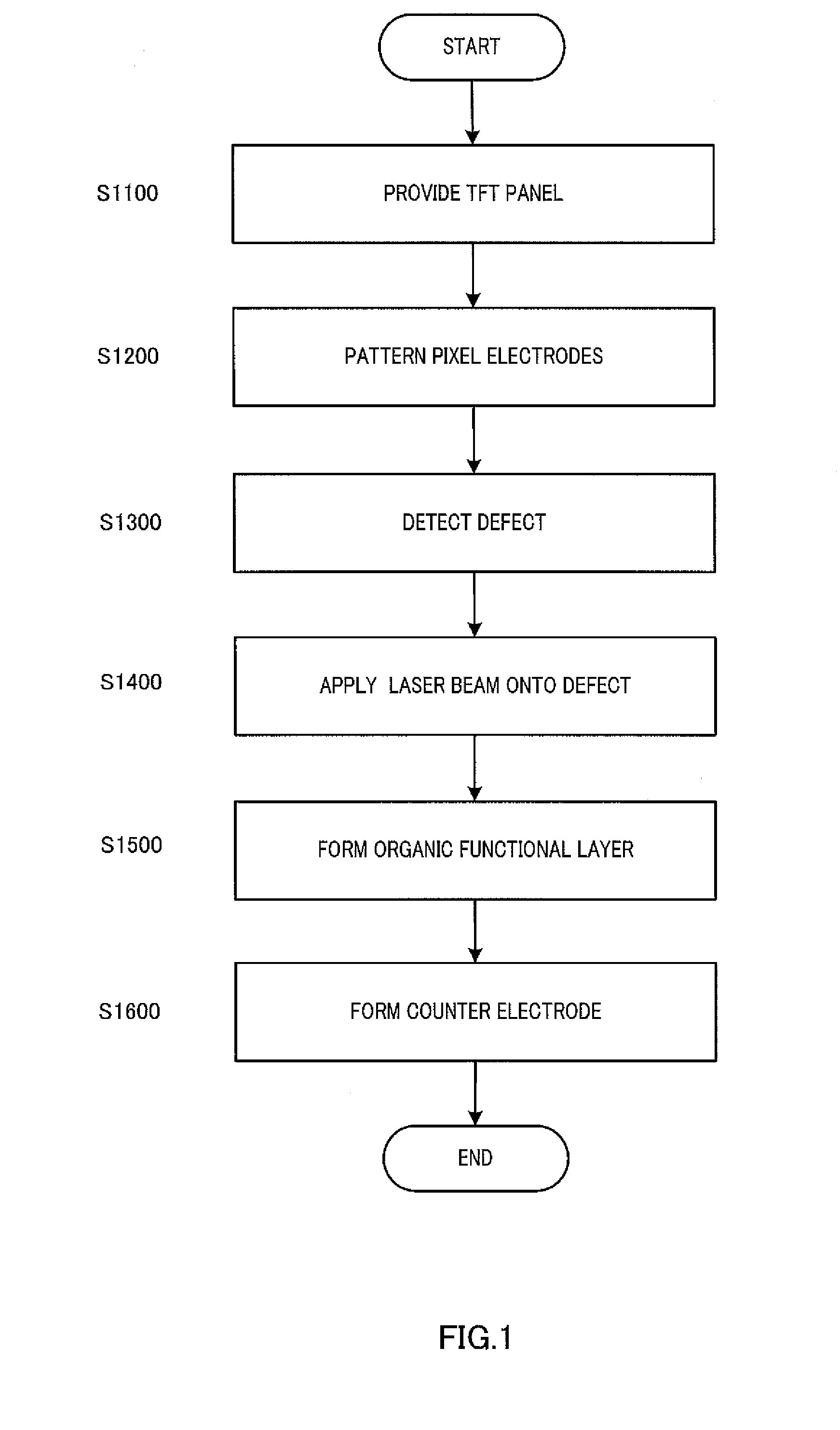
1. Method of Manufacturing Organic EL Panel

[0050]The present invention is effective particularly for the manufacture of large-screen organic EL panels. The reason for this is that manufacture of large-screen organic EL displays suffers from high risk of generation of defects in the pixel electrodes and therefore it is highly necessary to lessen luminance reductions caused by such defects. A manufacturing method according to an embodiment of the present invention will now be described with reference to the flowchart depicted in FIG. 1.

[0051]As seen from the flowchart depicted in FIG. 1, the manufacturing method according to an embodiment of the present invention includes: 1) a first step of providing a TFT panel (S1100); 2) a second step of patterning pixel electrodes on a surface of the TFT panel (S1200); 3) a third step of detecting in the pixel electrodes any defect in which the surface of the TFT panel is exposed (S1300); 4) a fourth step of roughening a surface of the TFT panel ...


PUM


Abstract

A local luminance reduction at defects in pixel electrodes with a rapid and easy method is achieved by providing a method of manufacturing an organic EL panel that includes a TFT panel and organic EL devices disposed over a surface of the TFT panel in matrix arrangement, each of the organic EL devices including: a pixel electrode disposed over the surface of the TFT panel, an organic luminescent layer disposed over the pixel electrode; and a counter electrode disposed over the organic functional layer.

Description

TECHNICAL FIELD[0001]The present invention relates to organic EL panels and methods of manufacturing the same.BACKGROUND ART[0002]An active matrix organic EL panel includes a TFT panel incorporated with thin-film transistors (TFTs) for controlling each individual sub-pixel, and organic EL devices disposed over the TFT panel.[0003]Each organic EL device used in organic EL displays generally includes a pixel electrode formed over the surface of the TFT panel; an organic functional layer disposed over the pixel electrode, which organic functional layer contains fluorescent molecules; and a counter electrode disposed over the organic functional layer.[0004]Recent increases in size and definition of organic EL panels has resulted in high probability of generation of defects in which portions of interconnects (e.g., pixel electrodes) on the TFT panel's surface are lost. For improved production yields, various approaches have been proposed that aim to repair such defects generated in the i...

Claims


Application Information

Patent Timeline
Patent Type & Authority Patents(United States)
IPC IPC(8): H01L51/52H01L51/56
CPCH01L27/3244H01L2251/568H10K71/861H10K59/1201H10K59/12
Inventor MIYAZAWA, KAZUTOSHI
Owner JOLED INC
Why Eureka
Try Eureka