Optical layer stack and method for manufacturing the same

a technology of optical layer and manufacturing method, which is applied in the field of optical layer stack, can solve the problems of deterioration of imaging quality, high manufacturing cost or little process yield, etc., and achieve the effect of reducing the cost of manufacturing additional needed spacer layers, less width, and less thickness

Active Publication Date: 2013-11-19
FRAUNHOFER GESELLSCHAFT ZUR FOERDERUNG DER ANGEWANDTEN FORSCHUNG EV
View PDF55 Cites 15 Cited by
  • Summary
  • Abstract
  • Description
  • Claims
  • Application Information

AI Technical Summary

Benefits of technology

[0014]Embodiments of the present invention thus on the one hand enable a housing concept for manufacturing opto-electronical mechanical systems in a panel, which decouples component and adjustment tolerances of mechanical components (spaces) from those of optically effective components (lens components). Thus, a cost advantage results in two respects: on the one hand costs in manufacturing additionally needed spacer layers are reduced. On the other hand, the yield of systems manufactured in the panel, i.e. on wafer-level, increases. The spacer layers or structures may further be manufactured in a cost-effective and lightproof polymer and eliminate conventionally needed additional components and manufacturing steps for preventing false light.

Problems solved by technology

This among others leads to high manufacturing costs or little process yield.
In both cases structures used for spacing the optically effective areas are transparent, which may be a disadvantage for the optical function as a result of the penetration of false light.
The different materials for layers having optically effective elements, spacer layers and joining layers are disadvantageous with respect to climate and long-term performance of the resulting optoelectronic system or the optical or optomechanical layer stack used therein.
When maintaining the spacing between lens and image, a defocusing and thus a deterioration of imaging quality results.

Method used


Image

  • Optical layer stack and method for manufacturing the same
  • Optical layer stack and method for manufacturing the same
  • Optical layer stack and method for manufacturing the same

Examples


Embodiment Construction

[0028]In the following description, in the different embodiments of the present invention like or seemingly like functional elements may comprise the same reference numerals. Thus, the description of those functional elements in the different embodiments illustrated in the following is interchangeable.

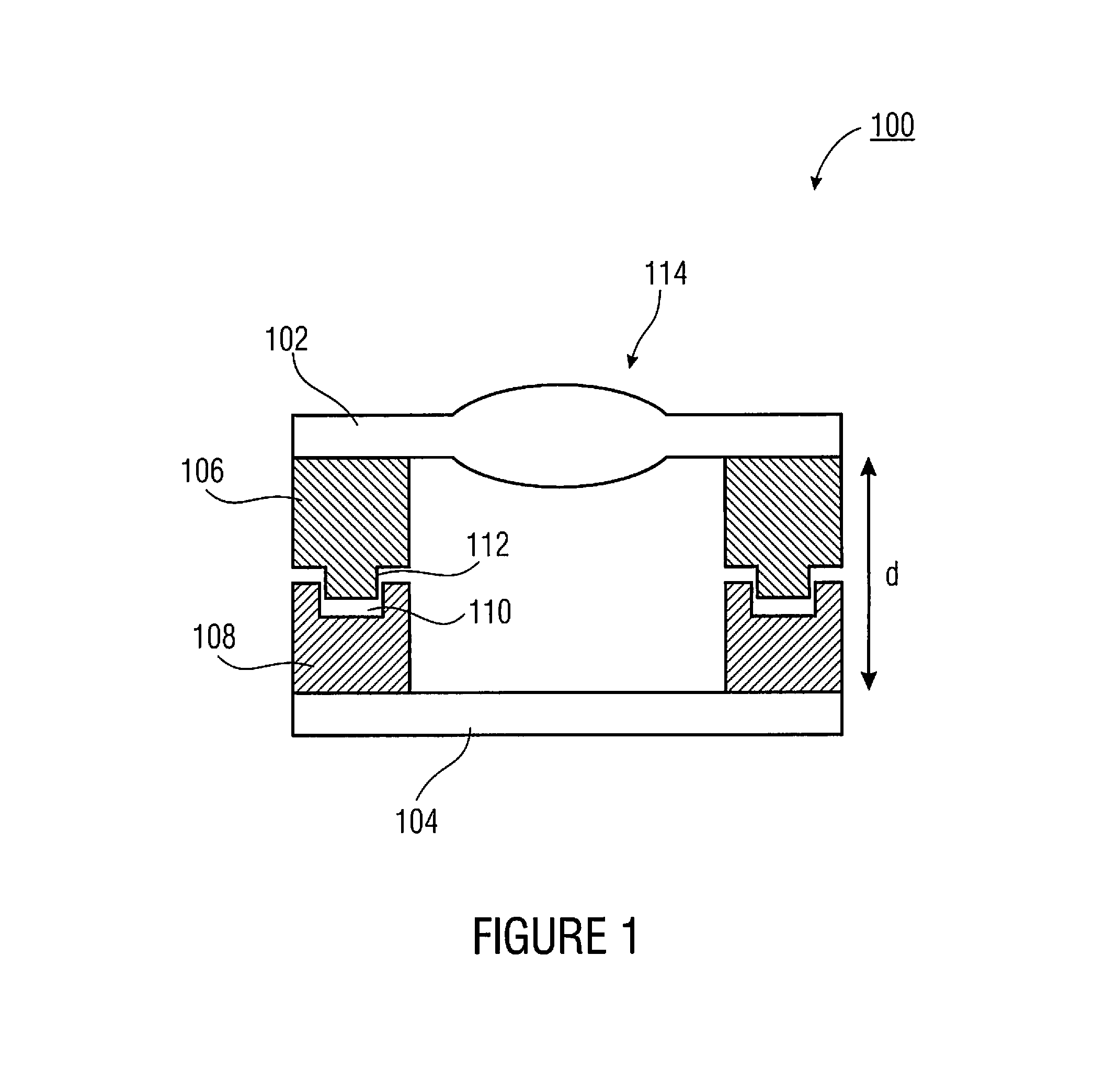
[0029]FIG. 1 schematically shows a side view of the optical or opto-mechanical layer stack 100 according to one embodiment of the present invention.

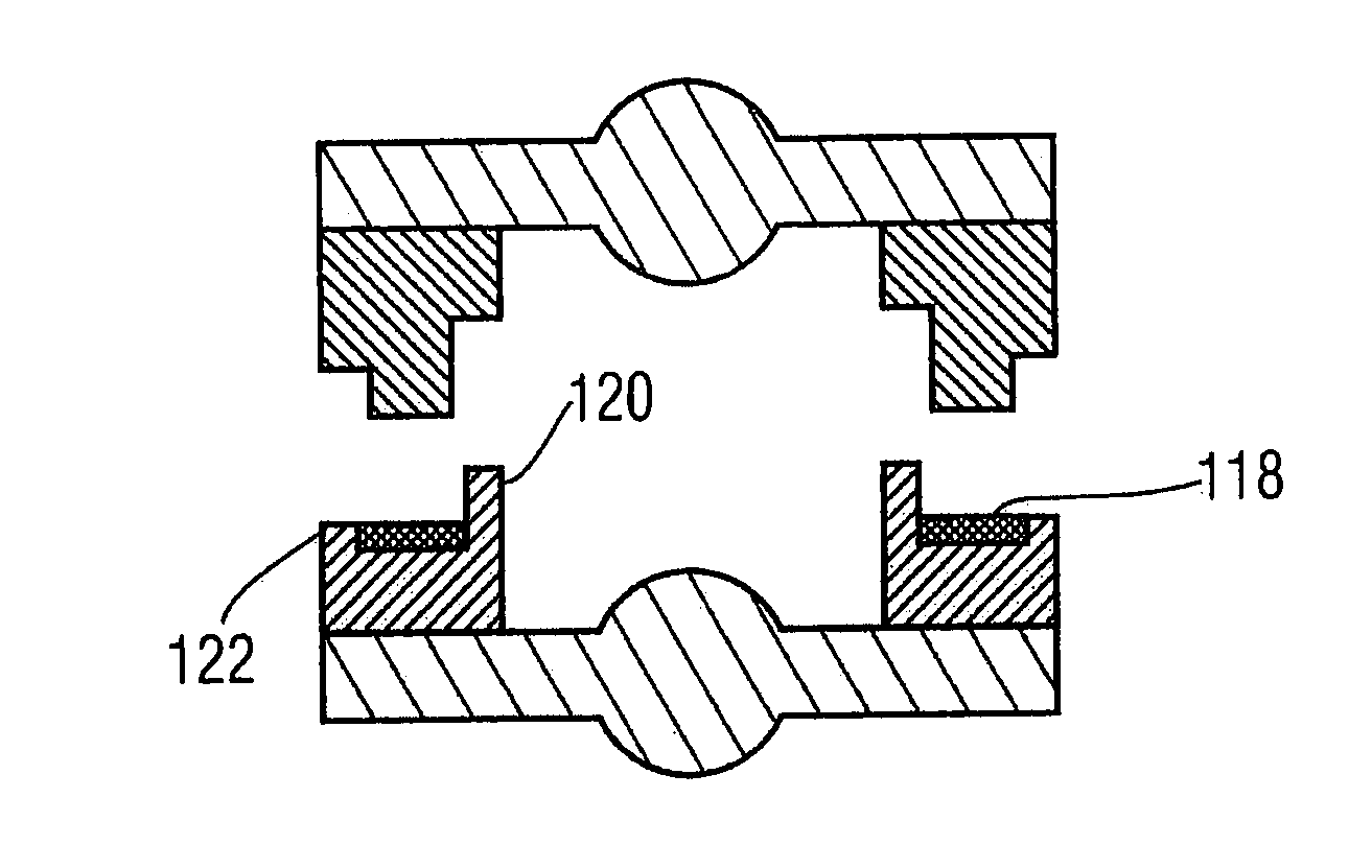
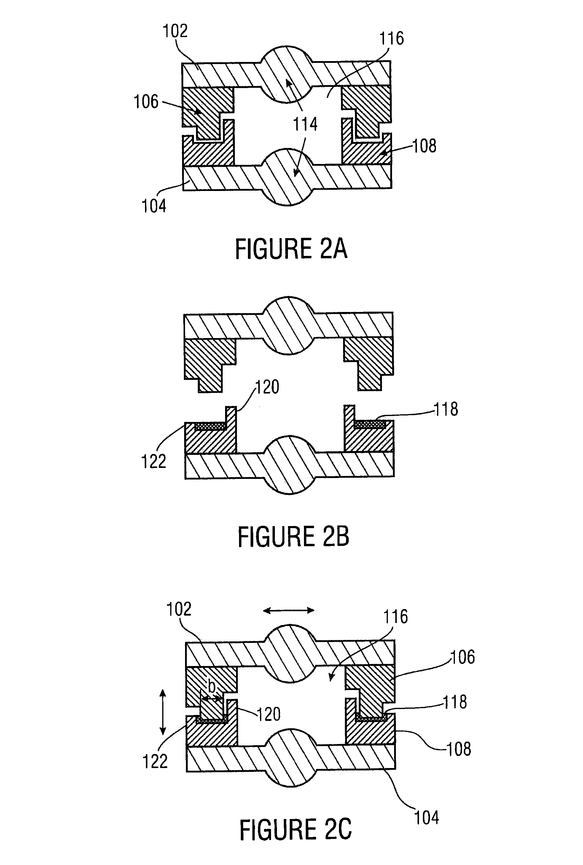
[0030]The optical layer stack 100 comprises a first layer 102 and a second layer 104. A first spacer part or portion 106 is associated with the first layer 102. A second spacer part 108 is associated with the second layer 104. The two spacer parts 106, 108 comprise groove 110 and tongue 112 for engaging in a stacking direction of the optical layer stack 100 in order to obtain a connection between the first spacer part 106 and the second spacer part 108 and a spacing of the first layer 102 and the second layer 104 in stacking direction.

[0031...


PUM

PropertyMeasurementUnit
temperatureaaaaaaaaaa
widthaaaaaaaaaa

Abstract

An optical layer stack having a first layer, a second layer, a first spacer part associated with the first layer and a second spacer part associated with the second layer, wherein the two spacer parts have groove and tongue for an engagement in a stacking direction of the optical layer stack in order to provide a connection between the first and the second spacer part and a spacing of the first and the second layer in stacking direction.

Description

CROSS-REFERENCE TO RELATED APPLICATIONS[0001]This application is a continuation of copending International Application No. PCT / EP2010 / 069779, filed Dec. 15, 2010, which is incorporated herein by reference in its entirety, and additionally claims priority from German Application No. DE 10 2009 055 083.6, filed Dec. 21, 2009, which is also incorporated herein by reference in its entirety.BACKGROUND OF THE INVENTION[0002]The present invention relates to an optical layer stack as it may, for example, be used for optoelectronic systems and, in particular, to the mechanical spacing of individual layers of the optical layer stacks.[0003]Optoelectronic systems or layer stacks as they are schematically illustrated in FIGS. 10a to 10c are, for example used in digital cameras, wireless devices having a photography function and many other applications. In the manufacturing of opto-electronic systems, e.g., micro objectives for mobile telephones, tight manufacturing and adjustment tolerances in ...

Claims


Application Information

Patent Timeline
Patent Type & Authority Patents(United States)
IPC IPC(8): G02B7/02G03B21/60B29D11/00G02B27/10
CPCG02B7/025G02B7/028
Inventor WIPPERMANN, FRANKDUPARRE, JACQUESDANNBERG, PETERBRAEUER, ANDREAS
Owner FRAUNHOFER GESELLSCHAFT ZUR FOERDERUNG DER ANGEWANDTEN FORSCHUNG EV
Why Eureka
Try Eureka