Active matrix substrate and display panel
a technology of active matrix substrate and substrate, applied in the direction of optics, instruments, transistors, etc., can solve the problems of liquid crystal material deterioration, and achieve the effect of reducing or preventing the increase in the number of manufacturing steps, reducing or preventing the diffusion of copper
- Summary
- Abstract
- Description
- Claims
- Application Information
AI Technical Summary
Benefits of technology
Problems solved by technology
Method used
Image
Examples
first embodiment
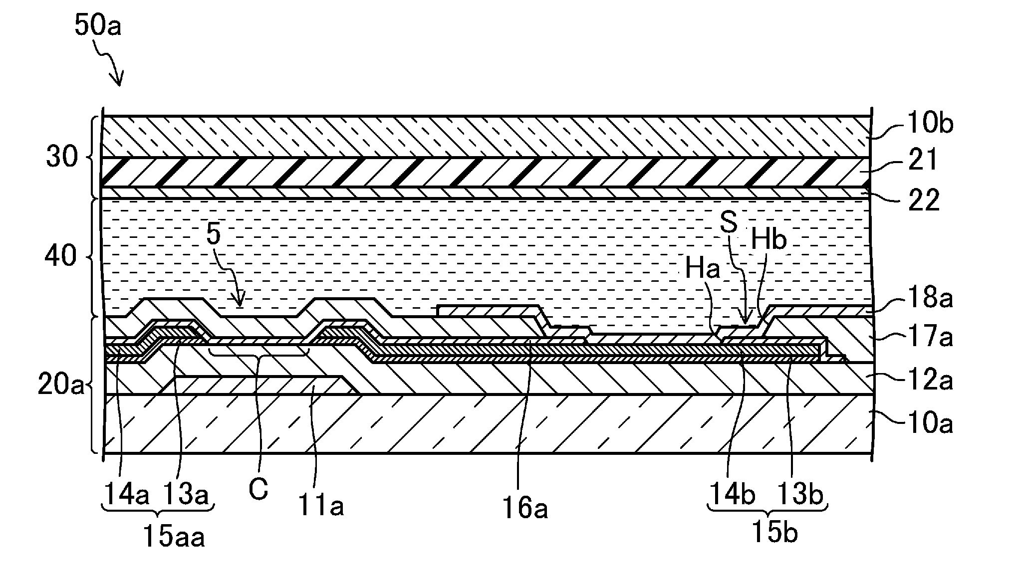
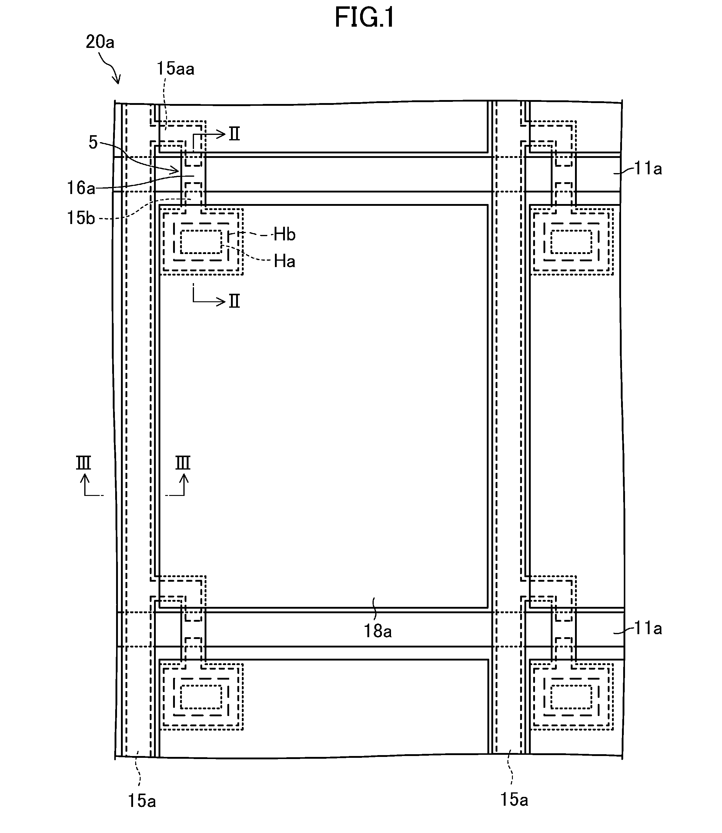
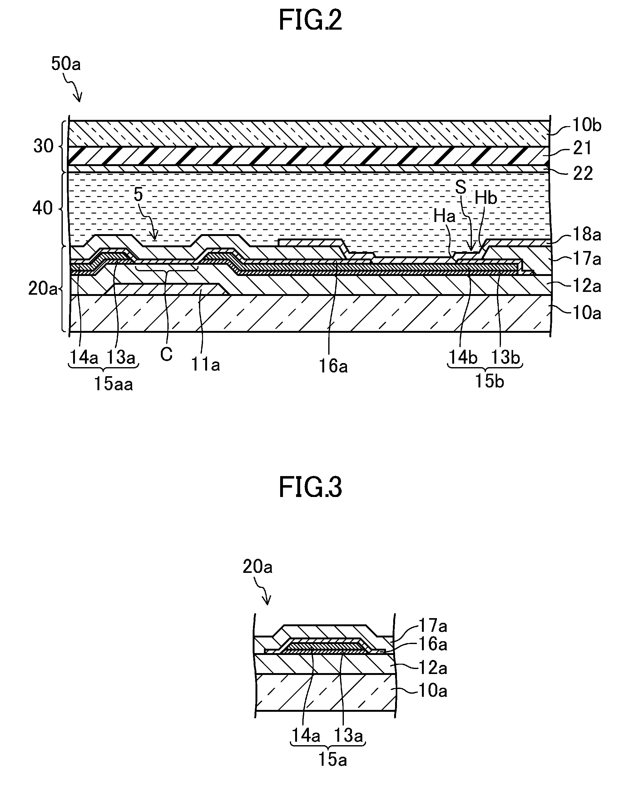
[0049]FIGS. 1-10 show an active matrix substrate and a display panel according to the present invention. Specifically, FIG. 1 is a plan view of the active matrix substrate 20a of this embodiment. FIG. 2 is a cross-sectional view of the active matrix substrate 20a and the liquid crystal display panel 50a including the active matrix substrate 20a, taken along line II-II of FIG. 1. FIG. 3 is a cross-sectional view of the active matrix substrate 20a, taken along line III-III of FIG. 1. FIG. 4 is a plan view of an interconnect terminal portion of the active matrix substrate 20a. FIG. 5 is a cross-sectional view of the interconnect terminal portion, taken along line V-V of FIG. 4. FIG. 6 is a plan view of an interconnect connection portion of the active matrix substrate 20a. FIG. 7 is a cross-sectional view of the interconnect connection portion, taken along line VII-VII of FIG. 6.
[0050]As shown in FIG. 2, the liquid crystal display panel 50a includes the active matrix substrate 20a and a...
second embodiment
[0092]FIGS. 11-18 show an active matrix substrate and a display panel according to the present invention. Specifically, FIG. 11 is a cross-sectional view of a liquid crystal display panel 50b including an active matrix substrate 20b of this embodiment. FIG. 12 is a plan view of an interconnect terminal portion of the active matrix substrate 20b. FIG. 13 is a cross-sectional view of the interconnect terminal portion, taken along line XIII-XIII of FIG. 12. FIG. 14 is a plan view of an interconnect connection portion of the active matrix substrate 20b. FIG. 15 is a cross-sectional view of the interconnect connection portion, taken along line XV-XV of FIG. 14. Note that, in the embodiments described below, the same parts as those of FIGS. 1-10 are indicated by the same reference characters and will not be described in detail.
[0093]In the first embodiment, the liquid crystal display panel has been illustrated which includes the active matrix substrate 20a on which the interlayer insulati...
PUM
| Property | Measurement | Unit |
|---|---|---|
| thickness | aaaaa | aaaaa |
| thickness | aaaaa | aaaaa |
| thickness | aaaaa | aaaaa |
Abstract
Description
Claims
Application Information


