
Organic light emitting display and driving method thereof

a technology of light-emitting diodes and organic light-emitting diodes, which is applied in the direction of electroluminescent light sources, static indicating devices, instruments, etc., can solve the problems of comparatively high cost, difficult to achieve the control method, and difficulty in large-scale or high-accuracy panels, so as to prevent non-uniformity and deviation of luminance, improve image quality, and detect quickly the effect of deterioration

Active Publication Date: 2013-12-03
SAMSUNG DISPLAY CO LTD
View PDF17 Cites 9 Cited by
  • Summary
  • Abstract
  • Description
  • Claims
  • Application Information

AI Technical Summary

Benefits of technology

This approach effectively prevents luminance non-uniformity and image sticking, ensures consistent display quality by compensating for transistor deviations and OLED deterioration, and enables real-time adjustment for maintaining desired luminance levels, including black luminance.

Problems solved by technology

The passive matrix type has the simple structure and a low cost, however it is difficult to realize a panel of a large size or high accuracy.
In contrast, with the active matrix type it is possible to realize a panel of a large size or high accuracy, however it is difficult to technically realize the control method thereof and a comparatively high cost is required.
However, the luminous efficiency is decreased by deterioration of the organic light emitting diode (OLED) such that the light emitting luminance is decreased for the same current.
The deterioration of the organic light emitting diode results in image sticking, and the characteristic deviation of the driving transistor results in mura.

Method used


Image

  • Organic light emitting display and driving method thereof
  • Organic light emitting display and driving method thereof
  • Organic light emitting display and driving method thereof

Examples


Embodiment Construction

[0056]The present invention will be described more fully hereinafter with reference to the accompanying drawings, in which exemplary embodiments of the invention are shown. As those skilled in the art would realize, the described embodiments may be modified in various different ways, all without departing from the spirit or scope of the present invention.

[0057]Constituent elements having the same structures throughout the embodiments are denoted by the same reference numerals and are described in a first embodiment. In the other embodiments, only constituent elements other than the same constituent elements will be described.

[0058]In addition, parts not related to the description are omitted for clear description of the present invention, and like reference numerals designate like elements and similar constituent elements throughout the specification.

[0059]Throughout this specification and the claims that follow, when it is described that an element is “coupled” to another element, ...


PUM


Abstract

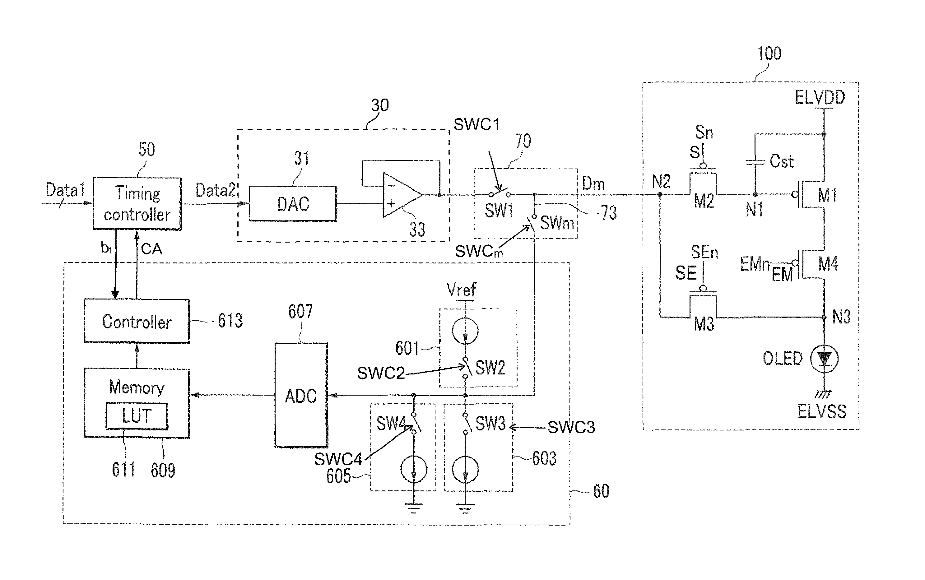
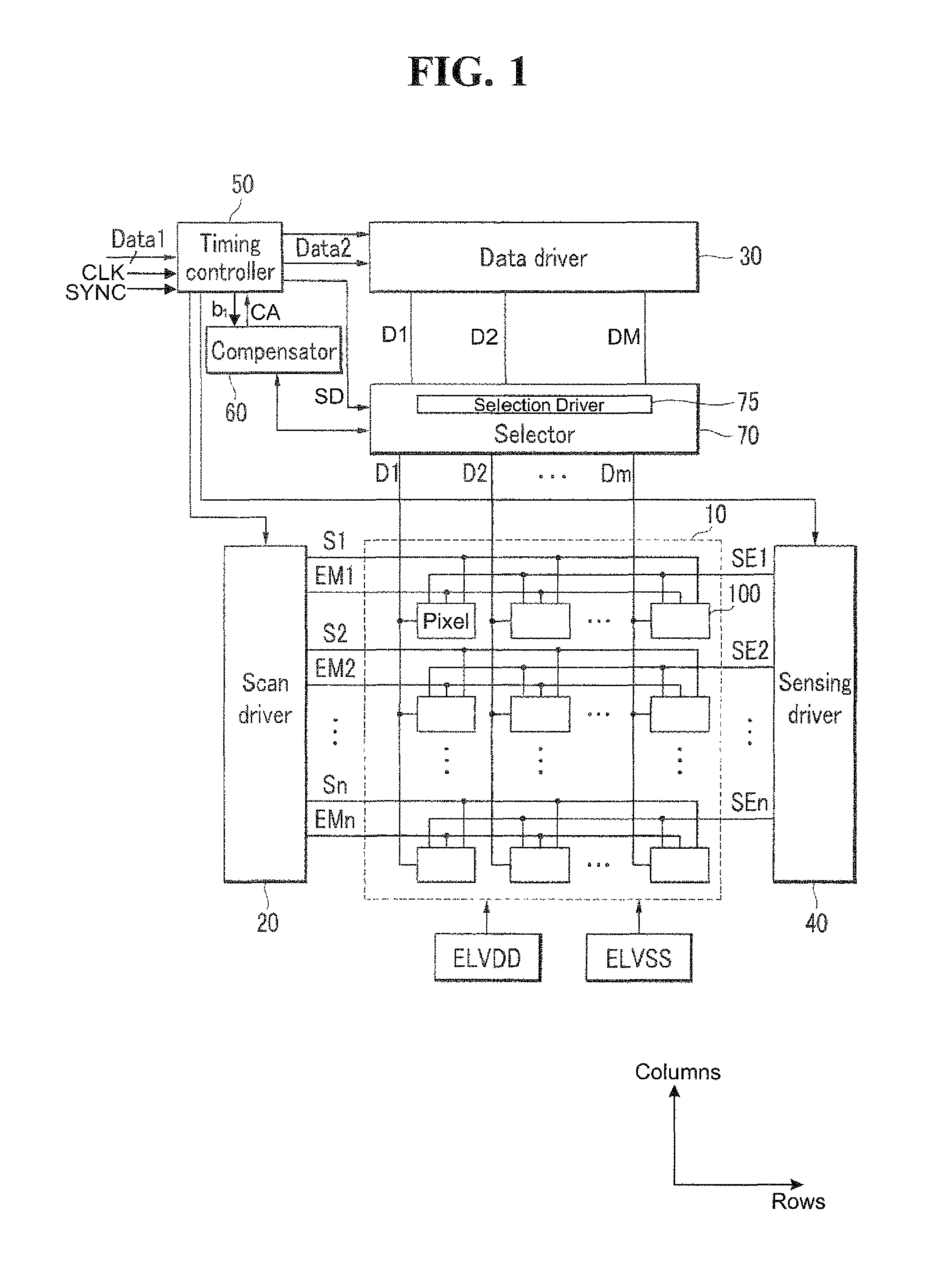
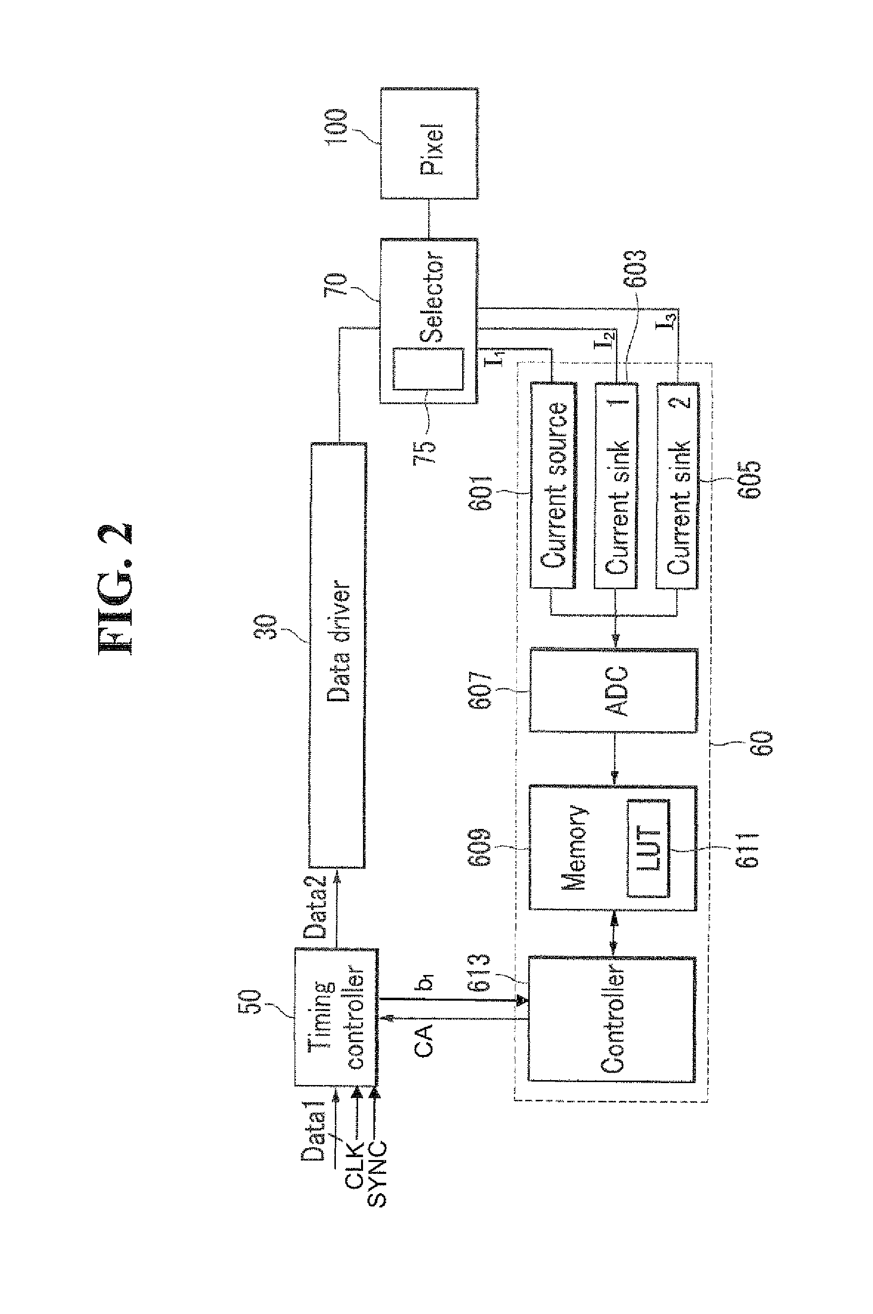
An organic light emitting diode (OLED) display comprises: an OLED; a driving transistor for supplying driving current to the OLED; a data line for transmitting a corresponding data signal to the driving transistor; a first transistor having a first electrode connected to one electrode of the OLED and a second electrode connected to the data line; and a second transistor having a first electrode connected to the data line and a second electrode connected a gate electrode of the driving transistor, wherein the first transistor, the second transistor, and the driving transistor are turned on, a first current and a second current are respectively sunk in a path of driving current from the driving transistor to the OLED through the data line, and a threshold voltage and mobility of the driving transistor are calculated by receiving a first voltage and a second voltage applied to the gate electrode of the driving transistor corresponding to sinking of the first current and the second current through the second transistor and the data line, and the data signal transmitted to the data line is compensated.

Description

CLAIM OF PRIORITY[0001]This application makes reference to, incorporates the same herein, and claims all benefits accruing under 35 U.S.C. §119 from an application earlier filed in the Korean Intellectual Property Office on Feb. 23, 2010 and there duly assigned Serial No. 10-2010-0016383.BACKGROUND OF THE INVENTION[0002]1. Field of the Invention[0003]The present invention relates to an organic light emitting diode (OLED) display and a driving method thereof. More particularly, the present invention relates to an organic light emitting diode display for quickly compensating deterioration of an organic light emitting diode and displaying an image with uniform luminance irrespective of a threshold voltage and mobility of a driving transistor, and a driving method thereof.[0004]2. Description of the Related Art[0005]Various kinds of flat display devices that are capable of reducing detriments of cathode ray tubes (CRT), such as their heavy weight and large size, have been developed in r...

Claims


Application Information

Patent Timeline
Patent Type & Authority Patents(United States)
IPC IPC(8): G09G5/10G09G5/00H05B44/00
CPCG09G3/3233G09G2320/0233G09G2320/0285G09G2320/0295G09G2320/043G09G2320/045
Inventor YOO, MYOUNG-HWANOH, CHOON-YULKWON, OH-KYONG
Owner SAMSUNG DISPLAY CO LTD
Learn More