Photosensitive detector with composite dielectric gate MOSFET structure and its signal readout method

a dielectric gate mosfet and photosensitive detector technology, applied in the field of imaging detectors, can solve the problems of inability to solve, low yield, and difficulty in increasing imaging speed

Inactive Publication Date: 2013-12-10
NANJING UNIV +1
View PDF6 Cites 18 Cited by
  • Summary
  • Abstract
  • Description
  • Claims
  • Application Information

AI Technical Summary

Problems solved by technology

Presently, CCD and CMOS-APS are widely used as imaging devices in scientific instruments and home imaging equipments, but they both have their shortcomings which cannot be resolved.
Its limitations are as follows.1) It is difficult to increase the imaging speed as CCD needs to transfer charges physically during imaging.2) The yield is low.
Because of the cascaded structure of MOS capacitors and the need of transferring charges, any failed MOS capacitor among a string of CCD pixel units can affect the transmission of charge and the following pixel units cannot work normally.
Therefore, process requirement for CCD manufacturing is very high, which usually leads to the low yield and high production cost.3) It is difficult to reduce the size of pixel unit further.
Therefore, the further scaling of the size of pixel unit is very difficult.
In addition, the edge effect also limits the further scaling of the pixel unit.
All of the limitations mentioned above are the essential problems of CCD, which can't be resolved fundamentally.

Method used


Image

  • Photosensitive detector with composite dielectric gate MOSFET structure and its signal readout method
  • Photosensitive detector with composite dielectric gate MOSFET structure and its signal readout method
  • Photosensitive detector with composite dielectric gate MOSFET structure and its signal readout method

Examples


Embodiment Construction

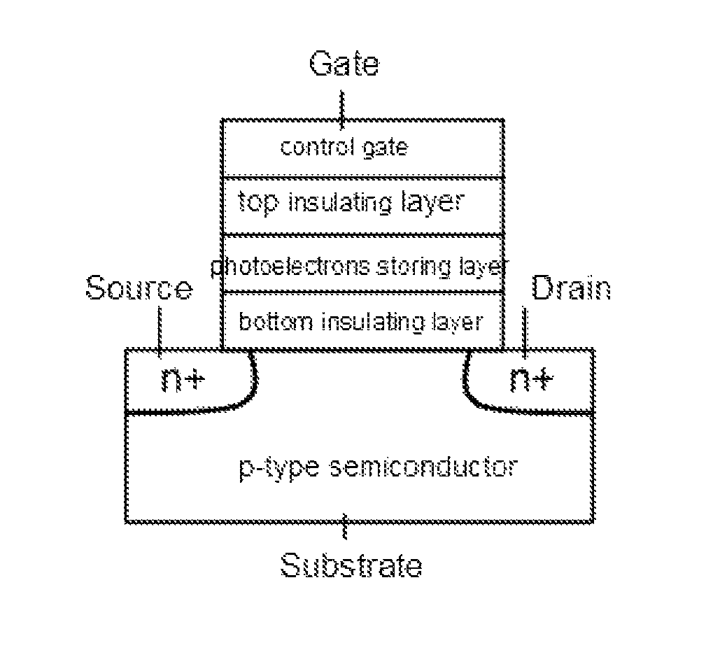
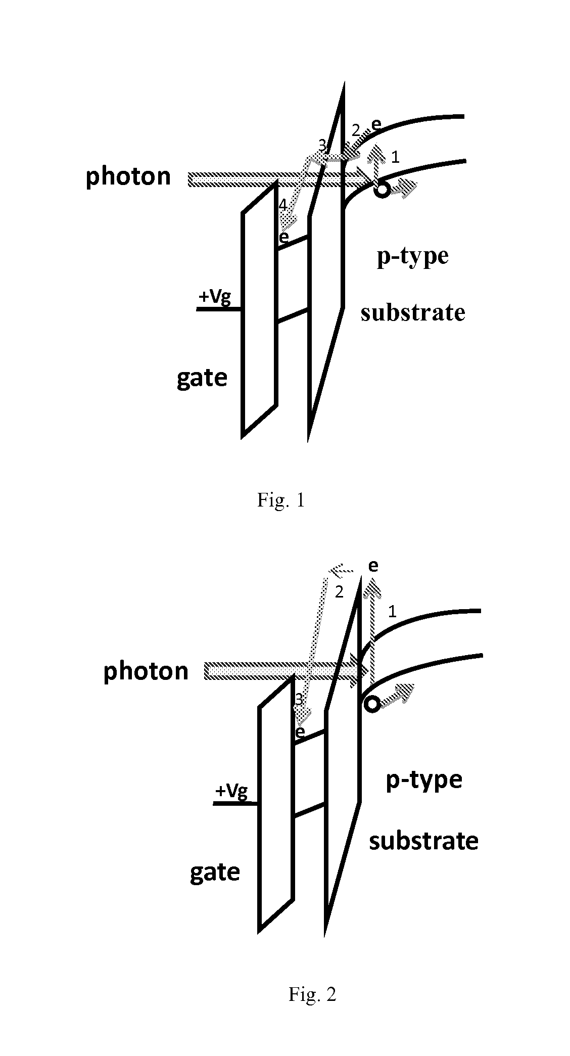
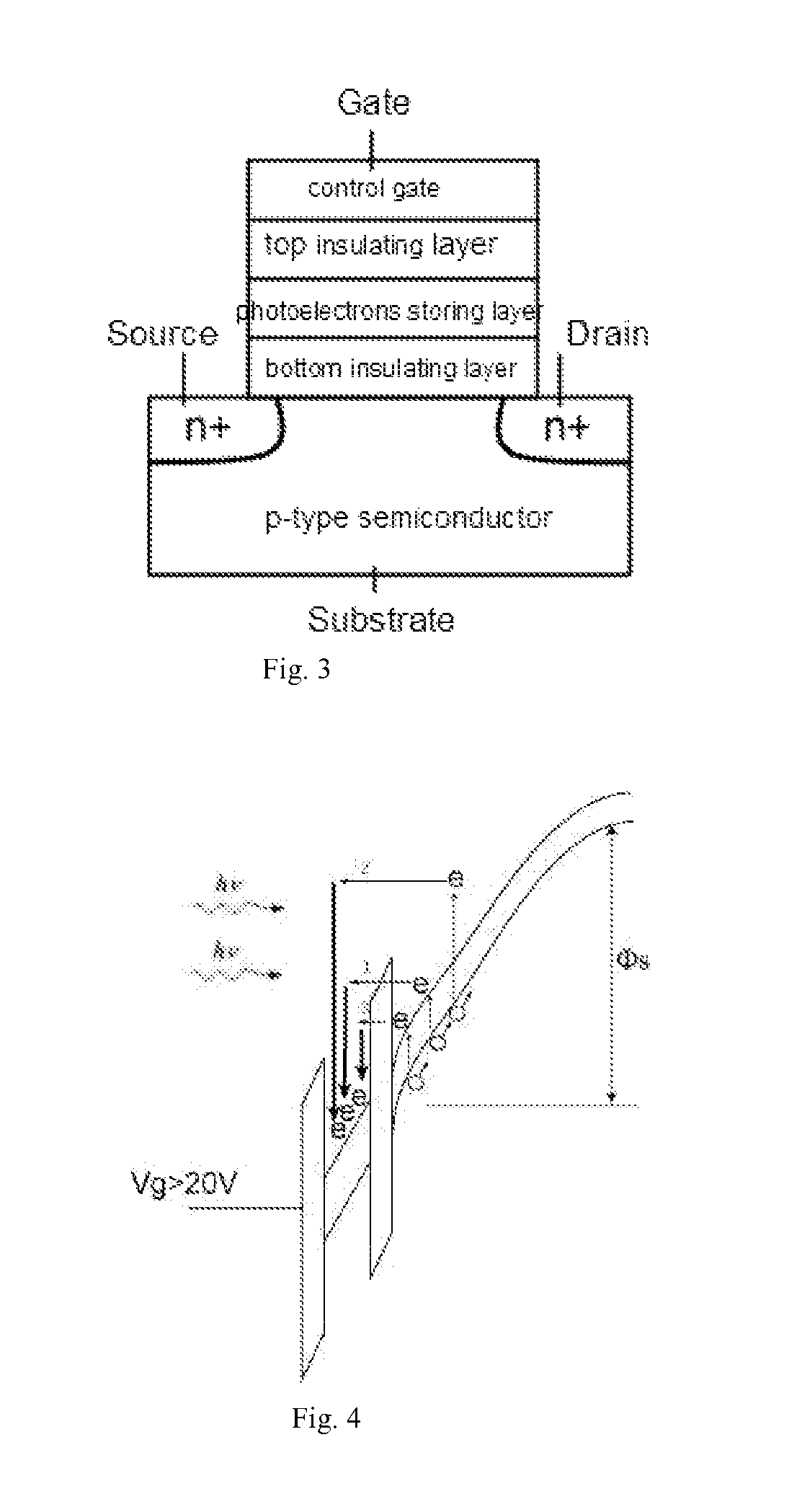
[0090]The Working Mechanism and Procedure of the Photoelectrons Storage Layer are as Follows:

[0091]1) Photoelectron Collection and Signal Acquisition:

[0092]Refer to the diagram of the energy band and photoelectrons generation and transfer in FIG. 1 and FIG. 2.

[0093]1. Photoelectron generation. If photon hv>semiconductor Eg (or Eg+ΔEc), photon will be absorbed by semiconductor, then electrons can be excited from valence band to conduction band.

[0094]2. Photoelectron transfer. If the gate voltage is higher than substrate voltage, the photoelectron will transfer to the interface between substrate and bottom dielectric. If the voltage difference between gate and substrate is positive voltage and photon hv>semiconductor Eg+ΔEc, the excited photoelectrons can enter photoelectron storage layer directly.

[0095]3. Photoelectron tunneling. The Photoelectron can tunnel into the photoelectron storage layer when the electric field in bottom dielectric is high enough.

[0096]4. Photoelectron storage...


PUM


Abstract

The present invention relates to a photosensitive detector with a composite dielectric gate MOSFET structure and its signal readout method. The MOSFET structure detector is formed on a p-type semiconductor substrate. N-type semiconductor regions locate on the two sides of the top part of the p-type semiconductor substrate to form a source and a drain. An underlying dielectric layer, a photo-electron storage layer, a top dielectric layer, and a control gate are stacked on the substrate in sequence. The top insulating dielectric layer can prevent the photoelectrons stored in the photo-electron storage layer from leaking into the control gate. The source and the drain are floating when photoelectrons are collected and injected into the photoelectron storing layer to be held therein. There is a transparent or semi-transparent window for detecting incident light forming on the substrate or gate surface. This invented detector has excellent scalability, basic compatibility with the flash memory fabricating technology, low leakage current, higher imaging speed than CCD, non-sensitivity to processing defects, larger dynamic range than other structures and higher accuracy of signal readout.

Description

CROSS REFERENCE TO RELATED PATENT APPLICATION[0001]The present application is the U.S. national stage of PCT / CN2010 / 070612 filed on Feb. 10, 2010, which claims the priority of the Chinese patent applications No. 200910024504.6 filed on Feb. 18, 2009, No. 200910030729.2 filed on Apr. 15, 2009 and No. 200910234266.1 filed on Nov. 18, 2009, which applications are incorporated herein by reference.FIELD OF THE INVENTION[0002]The present invention relates to an imaging detector working at infrared, visible light and ultraviolet band, mainly includes its structure, working principle and signal readout method. The invention describes a kind of photosensitive detector with a composite dielectric gate MOSFET structure and its signal readout method.BACKGROUND OF THE INVENTION[0003]Currently, CCD and CMOS-APS are the mainstream imaging detectors. The basic working principle of CCD is similar to the physical mechanism of metal-oxide-semiconductor (MOS) capacitor. CCD is consisted of MOS capacito...

Claims


Application Information

Patent Timeline
Patent Type & Authority Patents(United States)
IPC IPC(8): H01L31/00
CPCH01L31/1136H01L27/14643H01L27/14614
Inventor YAN, FENGZHANG, RONGSHI, YIPU, LINXU, YUEWU, FUWEIBO, XIAOFENGXIA, HAOGUANG
Owner NANJING UNIV
Why Eureka
Try Eureka