Optical element and light-emitting device

a technology of optical elements and light-emitting devices, which is applied in the direction of lighting and heating apparatus, planar/plate-like light guides, instruments, etc., can solve the problem of insufficient light-emitting area, and achieve the effect of reducing the size of the device and widening the light-emitting area

Inactive Publication Date: 2013-12-31
NITTO OPTICAL CO LTD +1
View PDF21 Cites 23 Cited by
  • Summary
  • Abstract
  • Description
  • Claims
  • Application Information

AI Technical Summary

Benefits of technology

[0010]Thus, it is an object of the present invention to provide an optical element and a light emitting device that makes it possible to widen a light illumination area despite a small-sized light emission area for downsizing the device.
[0019]It is preferable that the further from the position of the side of the light emitting component toward the distant position a location is, the greater gradually either of the incident angle of light entering the reflective surfaces of the saw teeth or the protrusion angle of the saw teeth is made at the location.
[0020]According to the present invention, provided can be an optical element and a light emitting device that makes it possible to widen a light illumination area despite a small-sized light emission area for downsizing the device.

Problems solved by technology

Unfortunately, in the case of such a plane lighting device described in Patent Document 1, directional characteristics of light are strong, and a light illumination area is not wide enough.

Method used


Image

  • Optical element and light-emitting device
  • Optical element and light-emitting device
  • Optical element and light-emitting device

Examples


Embodiment Construction

[0042]Structures and functions of an optical element and a light emitting device according to an embodiment of the present invention are described below with reference to the accompanied drawings.

[0043](Structure of Optical Element)

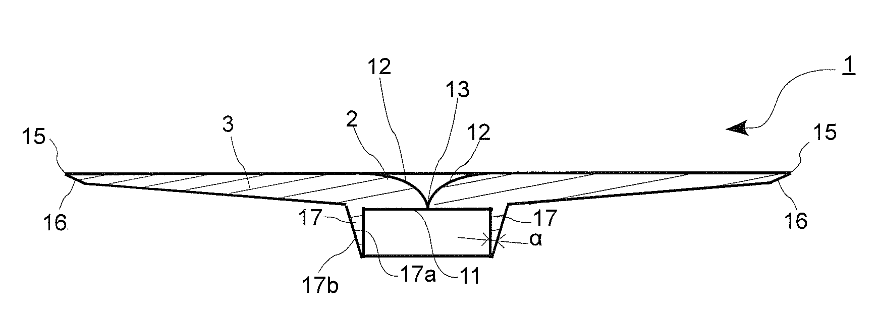
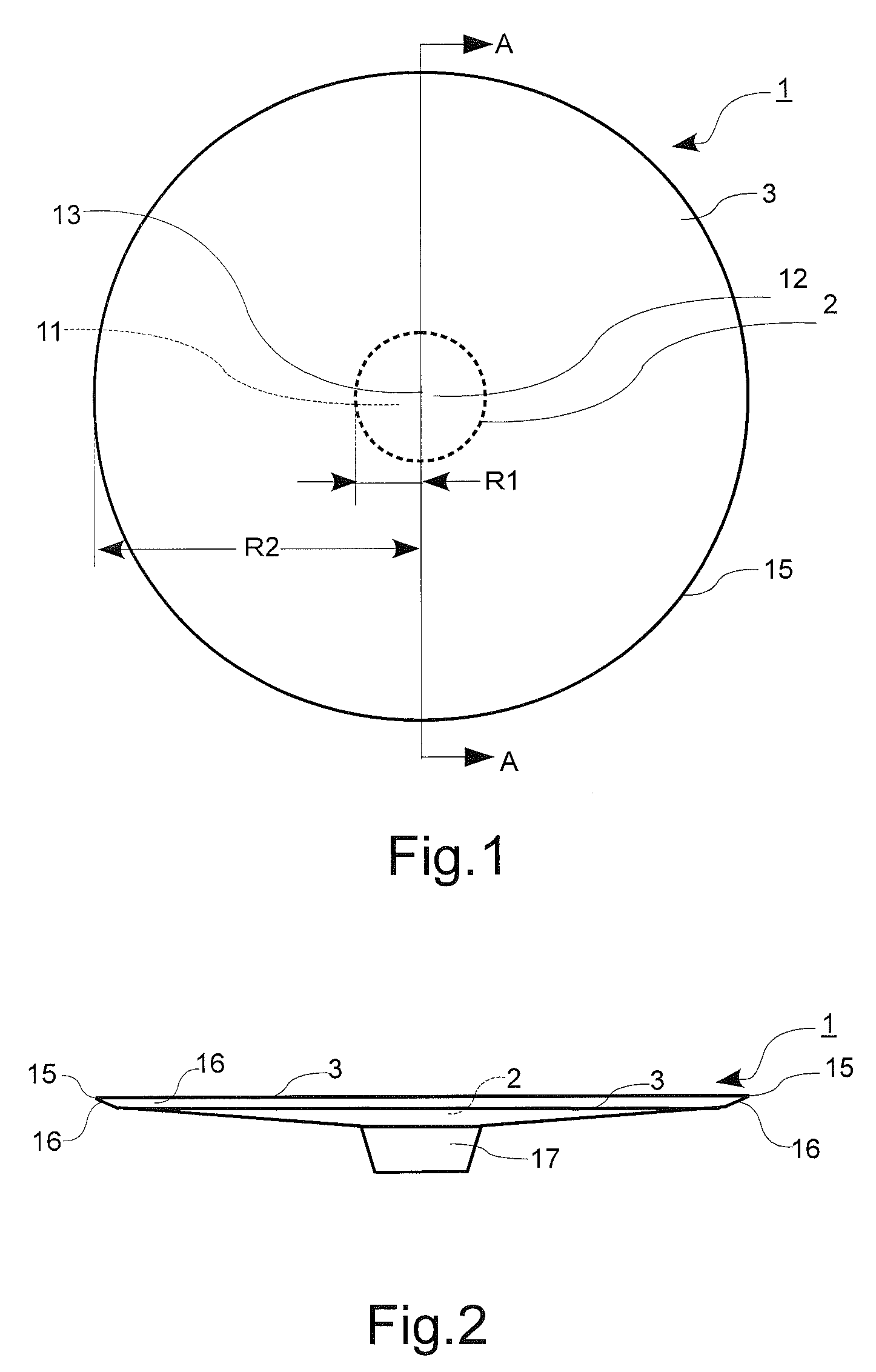
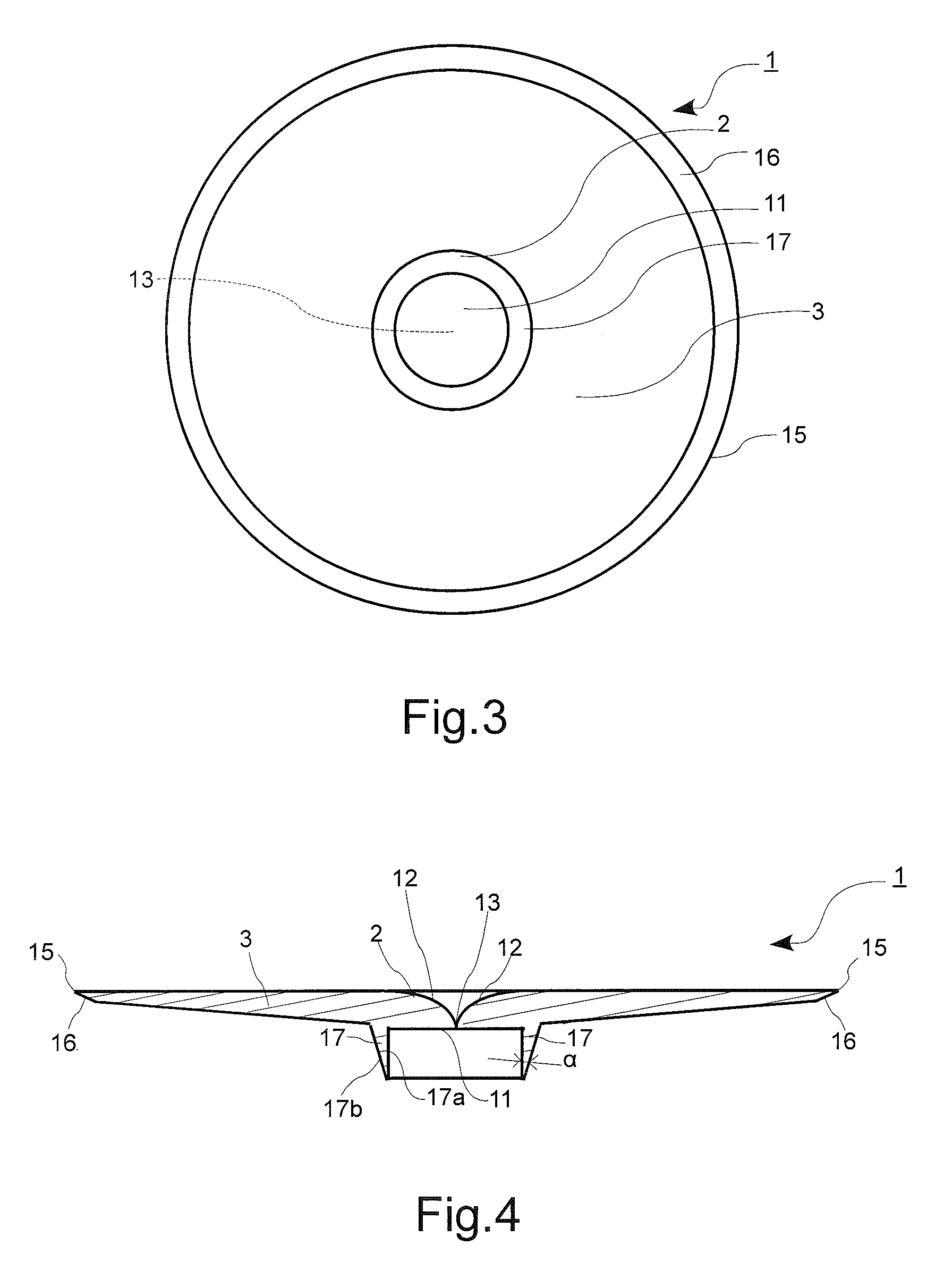
[0044]FIG. 1 is a plan view drawing to shows a structure of a translucent member 1 as an optical element according to an embodiment of the present invention, and in the meantime, FIG. 2 and FIG. 3 are a front elevation view and a bottom plan view of the translucent member, respectively.

[0045]As shown in FIGS. 1 to 3, having its circular contour, the translucent member 1 is a transparent poly-methyl methacrylate (hereinafter abbreviated to “PMMA”) resin compact that contains spherical and translucent silicone particles (not illustrated) with their particle diameter of several micro-meters, as light scattering particles. The translucent member 1 includes a first light guiding section 2 positioned at a central area, and being flat and circular-shaped; and a ...


PUM


Abstract

Provided are an optical element and a light-emitting device with which the illuminated area can be expanded in spite of a small light-emitting area, and that also enable the device to be downsize. The light-emitting device is equipped with sheet-like light-guide sections (a first light-guide section and a second light-guiding section) for guiding light, and a light-emitting member for emitting light. The second light-guide section has a prism section with a saw tooth-like cross-section for changing the direction of the light guided to one of its surfaces. In the prism section, the angle of incidence at which parallel light guided to the second light guide section enters reflective surface of saw teeth at positions away from the LED is set to be greater than the angle of incidence (δ) at which the light enters the reflective surface of the saw teeth at the side toward the LED. In addition, in the prism section, the angle of protrusion of the saw teeth at positions away from the LED is set to be greater than the angle of protrusion of the saw teeth at the side toward the LED.

Description

CROSS REFERENCE TO RELATED APPLICATIONS[0001]This is a U.S. national stage application of International Application No. PCT / JP2009 / 006157, filed on Nov. 17, 2009. Priority under 35 U.S.C. 119(a) and 35 U.S.C. 365(b) is claimed from Japanese Application No. JP 2008-294059, filed Nov. 18, 2008, the disclosure of which is also incorporated herein by reference.BACKGROUND OF THE INVENTION[0002]1. Field of the Invention[0003]The present invention relates to an optical element and a light emitting device.[0004]2. Description of Related Art[0005]In these years, LED lighting devices are coming into practical use in accordance with the development of high power LEDs (Light Emitting Diodes) and high efficiency LEDs as alternatives to incandescent light-bulbs and fluorescent lamps. Being compared with an incandescent light-bulb and a fluorescent lamp, an LED is small in its size and high in the luminous density. Furthermore, while the incandescent light-bulb and fluorescent lamp emit light in a...

Claims


Application Information

Patent Timeline
Patent Type & Authority Patents(United States)
IPC IPC(8): A45D42/10
CPCG02B6/0021G02B6/0041G02B6/0038G02B6/0018
Inventor SHINOHARA, YOSHINORI
Owner NITTO OPTICAL CO LTD
Why Eureka
Try Eureka