Display device and method of driving the same

a display device and active matrix technology, applied in the field of active matrix image display devices, can solve the problems of increasing the number of transistors, unable to cope with the increase of the screen size, and reducing the yield

Active Publication Date: 2014-01-21
JOLED INC
View PDF37 Cites 1 Cited by
  • Summary
  • Abstract
  • Description
  • Claims
  • Application Information

AI Technical Summary

Benefits of technology

[0011]Accordingly, it is possible to detect the threshold voltage of the drive transistor using three transistors per luminescence pixel, without scanning the power line, and to cause the luminescence element to produce light with the threshold voltage of the drive transistor being compensated. In this manner, the variation in the threshold voltage of the drive transistors is compensated, and thus luminance unevenness can be overcome.
[0040]As described above, the display device according to the present invention can compensate the threshold voltage the drive element using a small number of elements and without performing the scanning of the power source line.

Problems solved by technology

However, the method in Non-Patent Reference 1 uses four transistors per pixel, and thus there is concern over a decrease in yield due to an increase in the number of transistors to be integrated following an increase in the size of a display.
However, with one-dimensional wiring, crosstalk, in which the periphery of a display image becomes dark, easily occurs due to a drop in power source line voltage that accompanies an increase in the size of the display, and thus there is the problem of not being able to cope with increased screen size.

Method used


Image

  • Display device and method of driving the same
  • Display device and method of driving the same
  • Display device and method of driving the same

Examples


embodiment 1

(Modification of Embodiment 1)

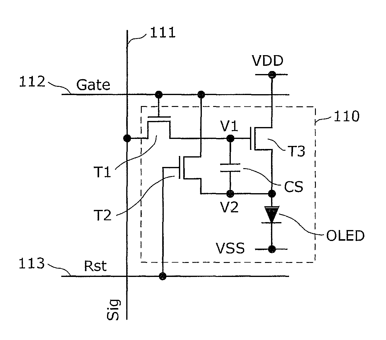
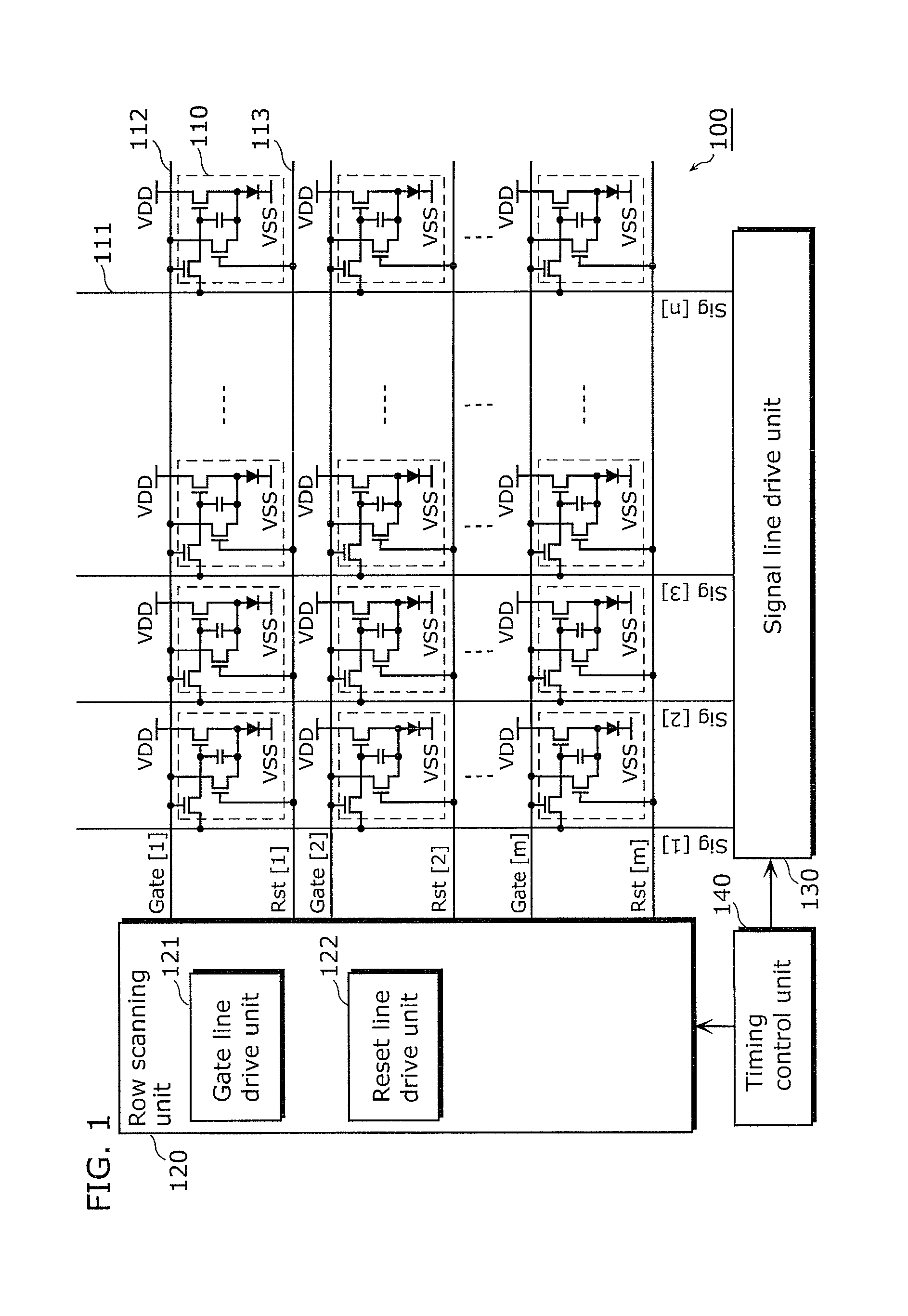
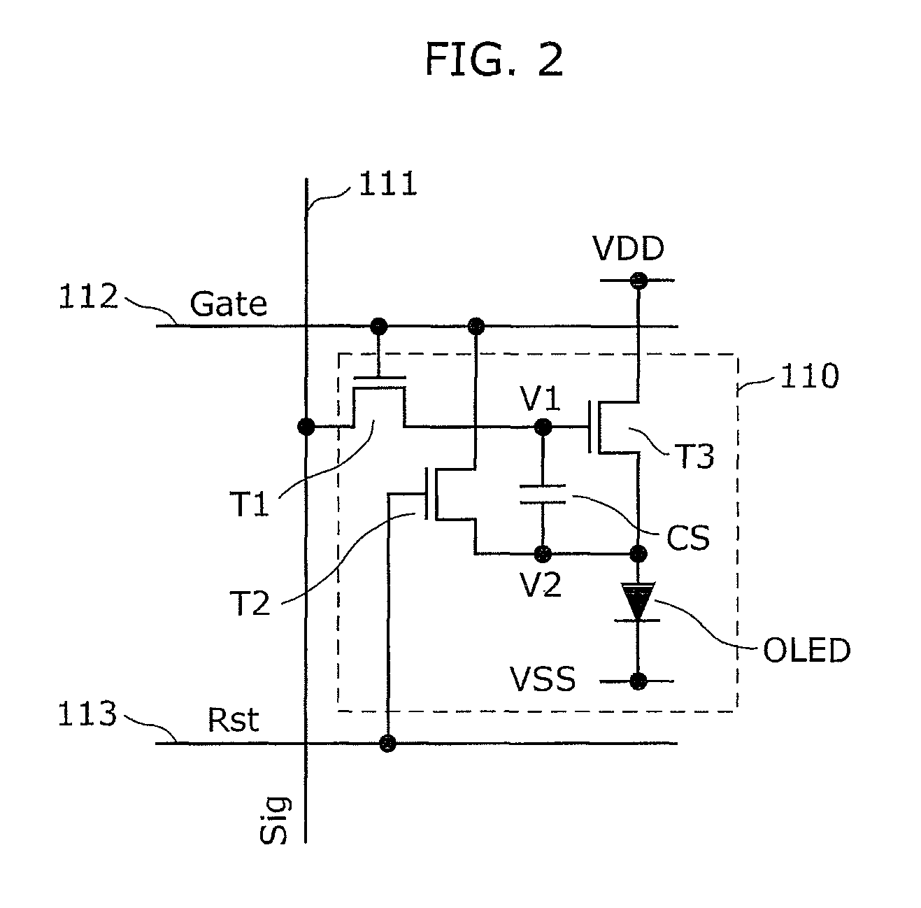
[0103]FIG. 5 is a timing chart showing the operation of the display device 100 when detecting the threshold voltage over plural horizontal periods. In the figure, time is indicated by the horizontal axis, and shown from top to bottom in the vertical direction are: a gate pulse Gate [1] applied to the gate line 112 corresponding to a luminescence pixel in the first row; a reset pulse Rst [1] applied to the reset line 113; the voltage waveform of V1 [1] of the pixel in the first row; the voltage waveform of V2 [1] of the pixel in the first row; the gate pulses Gate [2] to Gate [6] of luminance pixels in the second to sixth rows, respectively; the reset pulses Rst [2] to Rst [6] of the luminance pixels in the second to sixth rows, respectively; and a signal line voltage Sig of the signal lines 111. It should be noted that the figure shows the timing chart corresponding to one column of luminescence pixels 110. Furthermore, among the gate pulses Gate [1] to...

embodiment 2

(Modification of Embodiment 2)

[0135]FIG. 9 is a timing chart showing the operation of the display device 200 when detecting the threshold voltage over plural horizontal periods.

[0136]Compared to the timing chart shown in FIG. 5, in the timing chart shown in the figure, the period required for resetting is one horizontal period. In this manner, by performing the preparatory operation for threshold voltage detection in half the time, the Vth detection period can be made into a longer period compared to that in Embodiment 1, and thus high precision threshold voltage compensation can be realized. It should be noted that although the Vth detection period is set to five horizontal periods in FIG. 9, the horizontal periods required for the Vth detection period need not be limited to five horizontal periods as long as sufficient time for detecting the threshold voltage Vth (TFT) of the drive transistor T3 is secured.

embodiment 3

[0137]The display device in Embodiment 3 is approximately the same as the display device 100 in Embodiment 1 but is different in that one of the source terminal and the drain terminal of the reset transistor and the other end of the capacitor element are connected to one of the source terminal and the drain terminal of the drive transistor via a predetermined element.

[0138]Specifically, compared to each of the luminescence pixels included in the display device 100 in Embodiment 1, each of the luminescence pixels included in the display device in the present embodiment further includes a second switching transistor including a gate terminal, a source terminal, and a drain terminal. One of the source terminal and the drain terminal of the second switching transistor is connected to one of the source terminal and the drain terminal of the reset transistor and to the other end of the capacitor element, and the other of the source terminal and the drain terminal of the second switching t...


PUM


Abstract

A display device includes luminescence pixels arranged in rows and columns. Each of gate lines and reset lines correspond to one of the rows, and signals lines each correspond to one of the columns. Each luminescence pixels includes a luminescence element, a switching transistor, a drive transistor which supplies current to the luminescence element, and a reset transistor. The reset transistor includes a gate terminal connected to a corresponding reset line, one of a source and drain terminal connected to a source or drain terminal of the drive transistor, and the other of the source and drain terminal connected to a corresponding gate line. A capacitor is connected between the gate terminal and the source terminal of the drive transistor.

Description

CROSS REFERENCE TO RELATED APPLICATION[0001]This is a continuation application of PCT Application No. PCT / JP2010 / 002858 filed on Apr. 21, 2010, designating the United States of America, the disclosure of which, including the specification, drawings and claims, is incorporated herein by reference in its entirety.[0002]The disclosure of Japanese Patent Application No. 2009-124735, filed on May 22, 2009, including the specification, drawings, and claims is incorporated herein by reference in its entirety.BACKGROUND OF THE INVENTION[0003]1. Field of the Invention[0004]The present invention relates to active matrix image display devices using a current-driven luminescence element such as an organic electroluminescence (EL) element, and so on.[0005]2. Description of the Related Art[0006]Although organic EL elements represent the gray scale through current control, active matrix organic EL display devices have the problem that, due to variation in threshold voltage in drive transistors whi...

Claims


Application Information

Patent Timeline
Patent Type & Authority Patents(United States)
IPC IPC(8): G09G5/00G09G3/30G06F3/038
CPCG09G2310/0262G09G3/3233G09G2300/0852G09G2310/0251G09G2320/0233G09G2320/043G09G2300/0842G09G2310/061G09G3/3266G09G2300/0819G09G3/20G09G3/30G09G3/32G09G3/3225G09G2320/00G09G2320/02G09G2320/0271
Inventor MATSUI, MASAFUMI
Owner JOLED INC
Why Eureka
Try Eureka