Manufacturing method of semiconductor device

A manufacturing method and semiconductor technology, applied in semiconductor/solid-state device manufacturing, electrical components, circuits, etc., can solve problems such as short circuit of devices, large difference in etching thickness, poor interface flatness, etc., and achieve the effect of improving performance

Active Publication Date: 2016-02-03
SEMICON MFG INT (SHANGHAI) CORP
View PDF5 Cites 0 Cited by
  • Summary
  • Abstract
  • Description
  • Claims
  • Application Information

AI Technical Summary

Problems solved by technology

However, because the depth of the trench 50 is relatively large, the interlayer dielectric layer 30 needs to be etched for a long time, so a large amount of etching by-products (Polymer) generated during the etching process stay in the trench 50, and gather in the middle region at the bottom of the trench 50, slowing down the etching speed of the middle region at the bottom of the trench 50, so that the etching speed at the edge region at the bottom of the trench 50 is greater than the etching speed at the middle region, after a long time of etching , leading to an increasing gap in etching thickness, leading to the formation of such figure 2 In the structure shown, the middle region at the bottom of the trench 50 has not reached the etching thickness, while the edge region at the bottom of the trench 50 has been etched into the substrate 10 below. Since the interface flatness at the bottom of the trench 50 is poor, subsequent The ultra-thick metal layer deposited in the trench 50 is easy to form voids, which affects the electrical connection characteristics of the ultra-thick metal interconnection layer, and even causes etching to penetrate the substrate 10, and the subsequently formed ultra-thick metal layer is deposited into the substrate 10. Lead to serious short circuit of the device, affecting the performance of semiconductor devices
[0004] In order to solve the above problems, the prior art adopts the method of simply increasing the thickness of the etch stop layer. However, excessively increasing the thickness of the etch stop layer 20 will greatly increase the overall dielectric constant of the interlayer dielectric layer 30, thereby affecting the semiconductor device. The dielectric capability also affects the performance of semiconductor devices

Method used


Image

  • Manufacturing method of semiconductor device
  • Manufacturing method of semiconductor device
  • Manufacturing method of semiconductor device

Examples


Embodiment 1

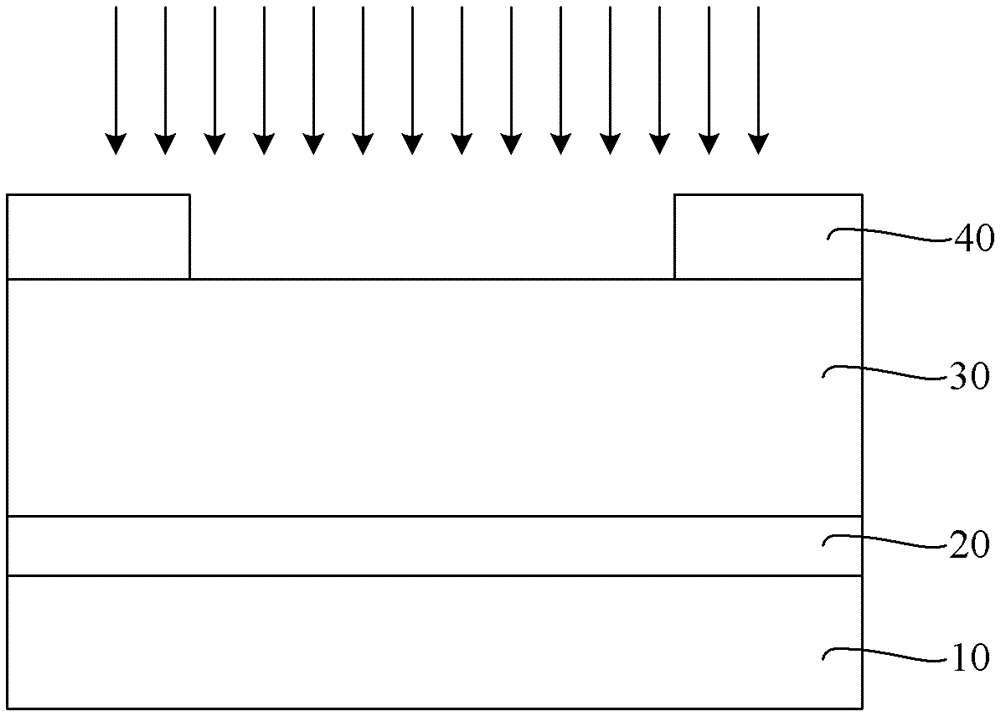
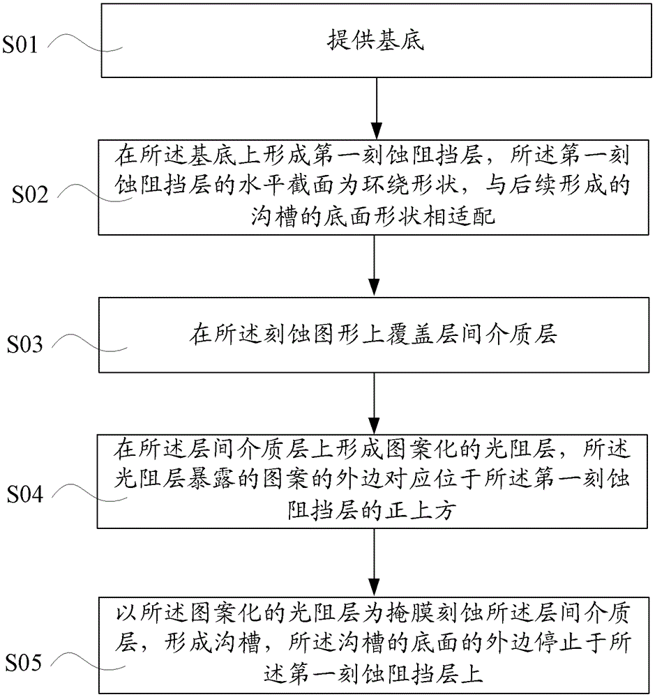
[0041] combine Figure 4 and Figure 5 , in step S01, a substrate 100 is provided, and the substrate 100 may be a semiconductor substrate with active circuits, or may be a previous metal interconnection layer.

[0042] continue to refer Figure 4 and Figure 5 , in step S02, first form a first etch barrier film (not shown in the figure) on the substrate 100, and use photolithography and etching processes to pattern the etch barrier film to form a first etch barrier layer 201, the horizontal cross-section of the first etch barrier layer 201 is in the shape of a circle, and the pattern formed around the first etch barrier layer 201 is adapted to the shape of the bottom surface of the subsequently formed trench, and the specific shape is formed according to needs The shape of the groove is determined, such as a circular ring or a "mouth", such as Figure 5 As shown, in this embodiment, taking the bottom of the groove as a rectangle as an example, the horizontal section of the...

Embodiment 2

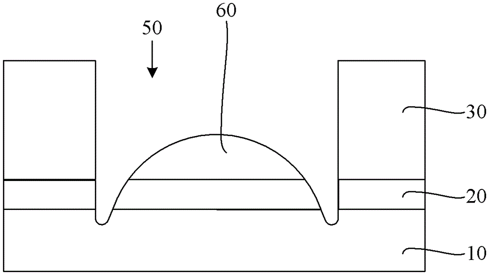
[0050] combine Figure 9 ~ Figure 11 , on the basis of Embodiment 1, in step S02, the sequence of forming the first etch barrier layer 202 and the second etch barrier layer 202 is changed; specifically, in this embodiment, the substrate 100 is first covered with the second The barrier layer 202, and then the first etch barrier film (not shown in the figure) is formed on the second etch barrier layer 202, and the first etch barrier film is patterned by photolithography and etching processes to form the first etch barrier film. layer 201, the first etch barrier layer 201 and the underlying second barrier layer 202 together form an etch barrier pattern 203; in this embodiment, the first etch barrier layer 201 is located at the second etch barrier On the layer 202, the thickness of the etch stop at the outer edge of the bottom surface of the trench is also thickened, so that when the trench 500 is formed by etching, it overcomes the problem that the etching removal rate near the o...

Embodiment 3

[0052] On the basis of Embodiment 2, in this embodiment, in step S02, a relatively thick etch stop film (not shown) is deposited first, and then the etch stop film is patterned to form a first etch stop layer 201 and The etching pattern of the second barrier layer 202 under it, the structure formed is the same as that described in Embodiment 2 Figure 11 The structure is the same. Specifically, combined with Figure 9 to Figure 11 Firstly, a thicker etching stopper film is formed on the substrate 100, and then part of the thickness of the etching stopper film is etched by photolithography and etching processes, and the etching time is controlled so that the etching stopper film is formed by the first etching process. The etch barrier layer 201 and the barrier pattern 203 formed by the second etch barrier layer 202 below it, the etch barrier pattern 203 formed by the covering deposition process combined with the etching process can also thicken the outer edge of the bottom sur...


PUM


Abstract

The invention provides a manufacturing method of a semiconductor device. A first etching barrier layer is formed on a substrate, the horizontal cross section of the first etching barrier layer is circle-shaped and matched with the shape of the bottom face of a groove formed in follow-up process, and therefore the thickness of an etching barrier pattern on the edge outside the bottom face of the groove is increased. In the process of etching to form the groove, the outer edge of the bottom face of the formed groove can stop at the first etching barrier layer, therefore the problem that the bottom face is uneven due to the fact that etching removing speed near the edge outside the groove is larger than the etching removing speed in the middle is solved, the substrate below the etching barrier layer is prevented from being damaged by etching, the phenomenon of short circuit of the device due to the fact that a super-thick metal layer enters the semiconductor substrate when the super-thick metal layer is formed in a deposition mode can be avoided, the super-thick metal layer which is good in electric connection characteristic can be formed in the follow-up process, and the performance of the semiconductor device can be improved.

Description

technical field [0001] The invention relates to a manufacturing method of a semiconductor device, in particular to a manufacturing method for forming a semiconductor device with an ultra-thick metal layer (UltraThickMetal). Background technique [0002] In the field of integrated circuit manufacturing, ultra-thick metal layers (UltraThickMetal) are widely used in semiconductor device structures with sizes ranging from 90nm to 65nm, and the thickness of the ultra-thick metal layer can reach more than 1000nm. [0003] Figure 1 to Figure 2 It is a structural schematic diagram of a manufacturing method of a semiconductor device in the prior art, such as Figure 1 to Figure 2 As shown, the process of making an ultra-thick metal layer includes: first forming an etching stopper layer 20 and an interlayer dielectric layer 30 on the substrate 10; then forming a patterned photoresist layer 40 on the interlayer dielectric layer 30, and forming The patterned photoresist layer 40 is use...

Claims


Application Information

Patent Timeline
Patent Type & Authority Patents(China)
IPC IPC(8): H01L21/311
Inventor 符雅丽王新鹏
Owner SEMICON MFG INT (SHANGHAI) CORP
Why Eureka
Try Eureka