A cavity type bulk acoustic wave resonator and its preparation method
A bulk acoustic wave resonator and cavity technology, applied in the direction of impedance network, electrical components, etc., can solve the problems of low film quality, cavity corrosion residue, etc., and achieve the effects of not easy to damage, high yield, and reducing clutter
- Summary
- Abstract
- Description
- Claims
- Application Information
AI Technical Summary
Problems solved by technology
Method used
Image
Examples
Embodiment 1
[0054] The method of preparing the cavity acoustic resonator of the present embodiment includes the following steps:
[0055] (a) take a substrate, the substrate is a single crystal silicon; an anisotropic etching method using silicon, a cavity layer that blocks the heat flow diffusion in single crystal silicon, specifically: on the substrate Transferring the graphics that needs to be etched, then prepared a mask on the surface of the substrate, and a convex angle compensation portion is provided at the convex angles of the mask, and then wet etching, the process of etching. In the case where the mask of the mask is retained, the portion that is not covered by the mask is etched away, forming a cavity; the wet etching can perform single crystal silicon anisotropic etching, due to When a wet etch etching single crystal silicon, the corrosion liquid will have the fastest corrosion rate below the "holes" structure in the mask pattern, so Figure 11 As shown, by etching graphical desig...
Embodiment 2
[0068] The method of preparing the cavity acoustic resonator of the present embodiment includes the following steps:
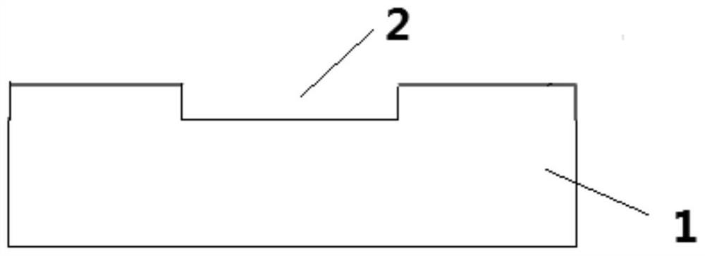
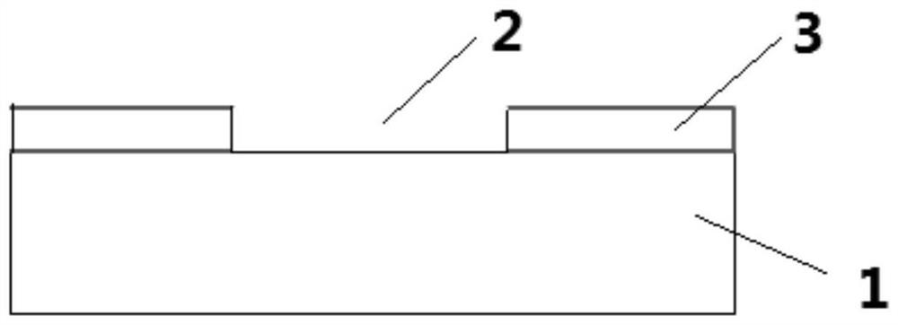
[0069](a) Repair the substrate, the substrate is single crystal silicon; a support film is grown on the substrate, and then the side of the growth support film is patterned, etching the support film, forming a cavity. The support film is SiO 2 . Such as figure 2 As shown, the structure of the substrate having a cavity obtained in step (a) is shown.
[0070] As the implementation of the present embodiment, the support surface and the substrate can also be etched.
[0071] (b) Repairing the electrical single crystal wafer, the piezoelectric single crystal wafer is a lithium chipylate wafer, and ion implantation is performed on the piezoelectric single crystal wafer, and the implanted ion is H ion, and the energy injected into ions. In 195kev, the injection dose is 6 × 10 16 / cm 2 1 μm / cm -2 The injection depth is 6 μm to obtain a heat removal material, and then, ...
Embodiment 3
[0077] The method of preparing the cavity vapor resonator of the present embodiment is prepared using the same method as in Example 1, and the difference is only that the bottom electrode is larger than the upper surface area of the cavity.
[0078] Such as Figure 8 As shown, a structural diagram of the extracted ion implantation obtained in step (b) and having a piezoelectric single crystal wafer of the bottom electrode.
[0079] Such as Figure 9 As shown, the structure is shown in the structural diagram of the side coating of the pressure single crystal wafer in step (c);
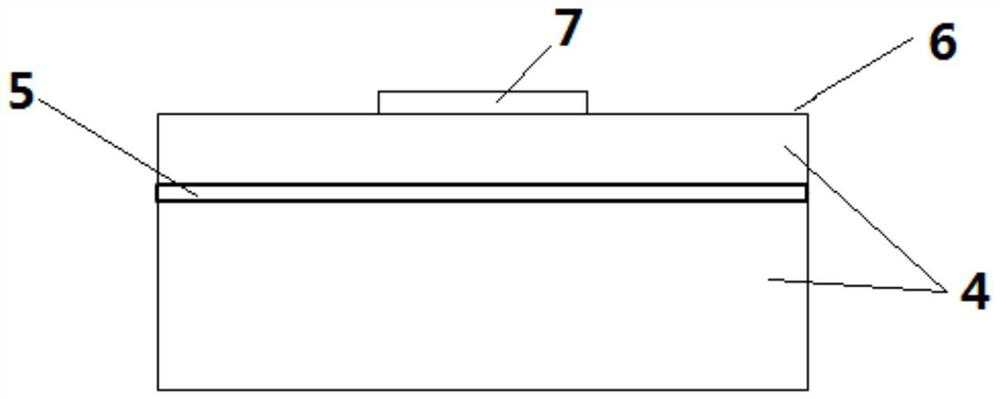
[0080] Figure 10 The structural diagram of the cavity body acoustic wave resonator in step (d) of the method of preparing a cavity acoustic resonator in Example 3 of the present invention.
PUM
| Property | Measurement | Unit |
|---|---|---|
| thickness | aaaaa | aaaaa |
| thickness | aaaaa | aaaaa |
| thickness | aaaaa | aaaaa |
Abstract
Description
Claims
Application Information


