Miniaturized substrate integrated waveguide circulator
A substrate-integrated waveguide and circulator technology, applied in the field of microwave technology, can solve problems such as large size and unfavorable integration, achieve high Q value, facilitate integration, and reduce volume
- Summary
- Abstract
- Description
- Claims
- Application Information
AI Technical Summary
Problems solved by technology
Method used
Image
Examples
Embodiment Construction
[0018] In the present invention, the metallized through hole forms a waveguide structure, and two composite graded microstrip lines are arranged in the waveguide, which enhances the matching performance of the device and is beneficial to the miniaturization and integration of the whole device.
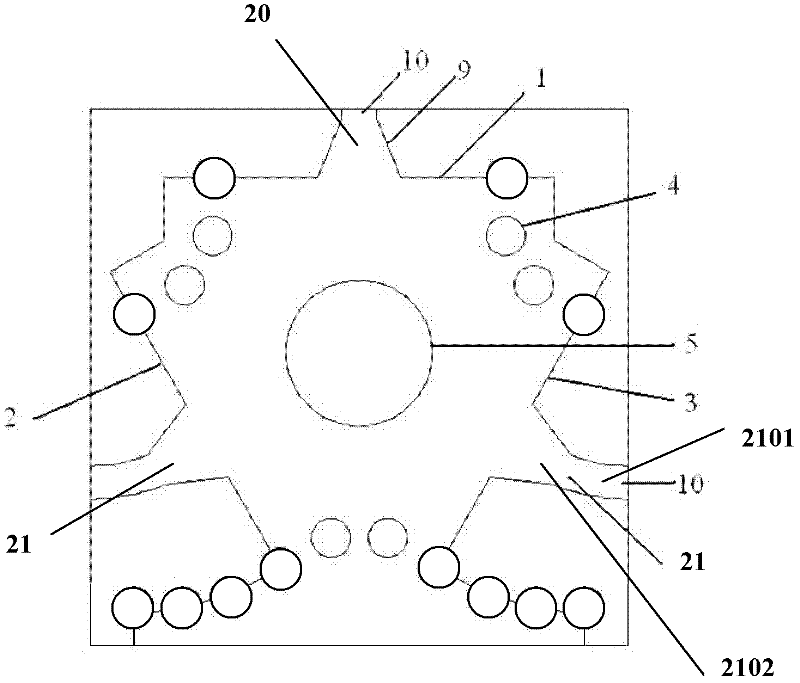
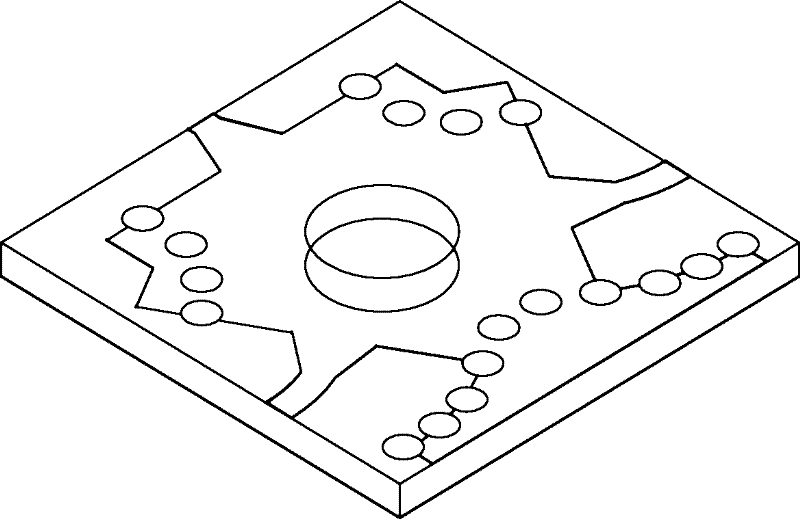
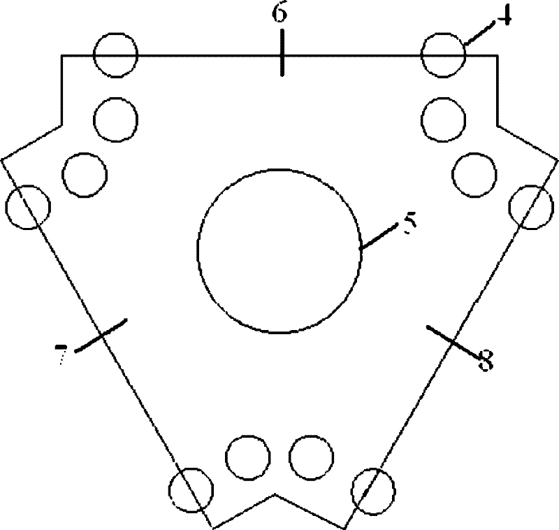
[0019] The present invention includes the central junction part of the circulator ( image 3 Shown) and the microstrip conversion connection part ( Figure 4 , 5 shown). The substrate of the entire circulator is a double-sided copper-clad high-frequency dielectric board Taconic CER-10, with a relative dielectric constant of 10, a loss tangent of 0.0035, and a thickness of 0.762mm.
[0020] image 3 It is the central junction part of the circulator, which is composed of three substrate-integrated waveguide structures (6-8) forming an angle of 120° and a central ferrite cylinder (5). The three substrate integrated waveguide structures are realized by opening metallized through holes ...
PUM
 Abstract
Description
Claims
Application Information


