Folding self-die substrate integrated waveguide
A half-mode substrate integration and waveguide technology, which is applied in the direction of waveguides, waveguide devices, printed circuit components, etc., can solve the problems of large size and achieve high Q value, low loss, and high Q value
- Summary
- Abstract
- Description
- Claims
- Application Information
AI Technical Summary
Problems solved by technology
Method used
Image
Examples
Embodiment 1
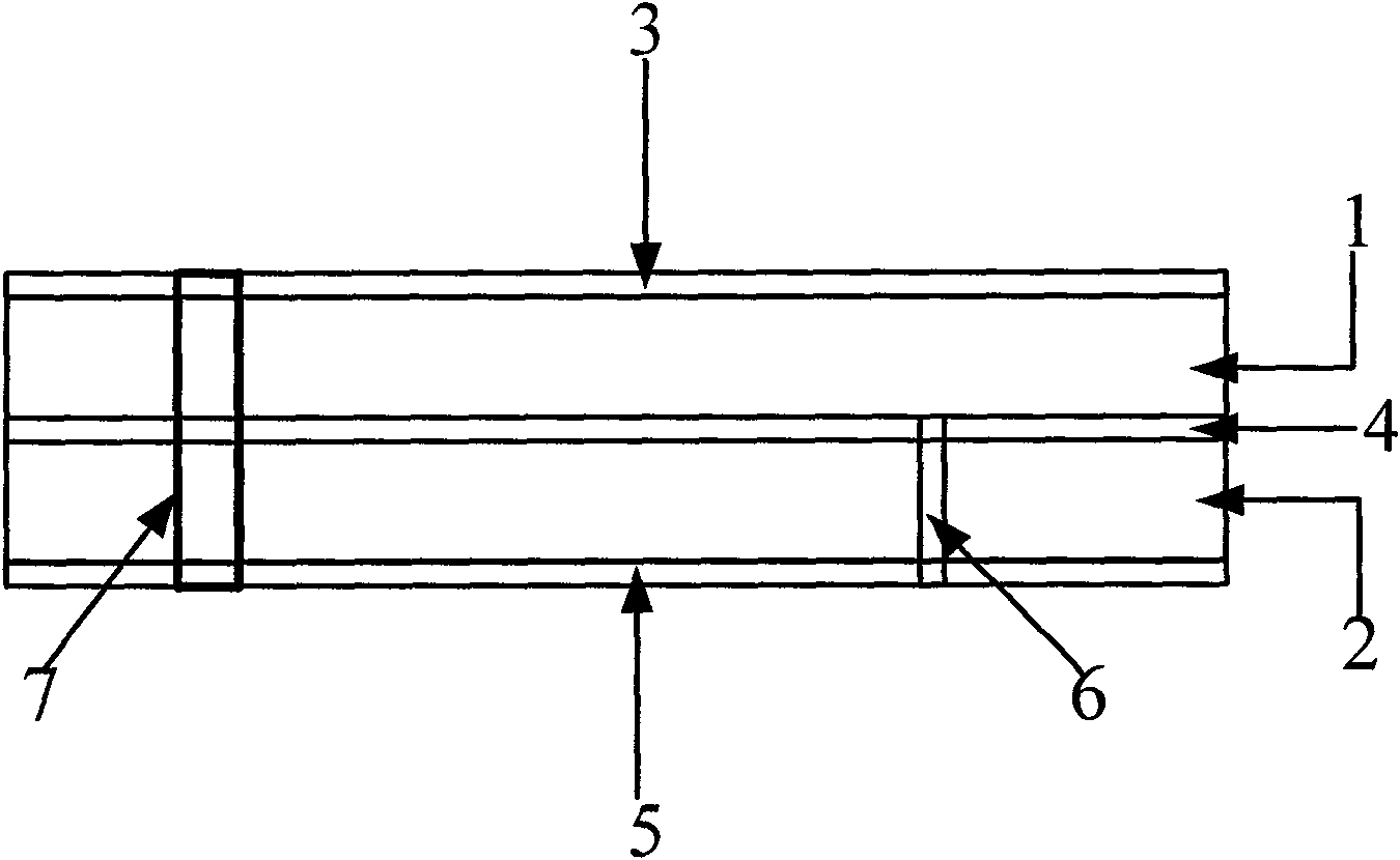
[0022] Embodiment 1 Folded half-mode substrate integrated waveguide
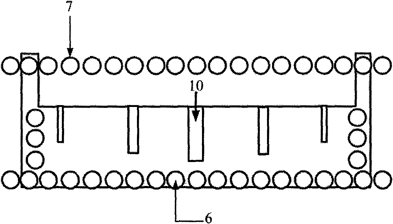
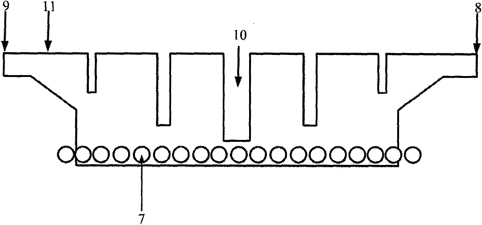
[0023] image 3 It is a folded half-mold substrate integrated waveguide with slots etched on the upper metal surface,
[0024] Figure 4 It is a folded half-mode substrate integrated waveguide with slots etched on the metal surface of the middle layer,
[0025] Figure 5 It is the actual test result of the first filter in the first embodiment of the present invention,
[0026] Image 6 It is the actual test result of the second filter in the first embodiment of the present invention,
[0027] Table 1 is the size of the first filter in Embodiment 1,
[0028] Table 2 shows the dimensions of the second type of filter in Embodiment 1.
[0029] Table I
[0030]
[0031] Table II
[0032]
PUM
 Abstract
Description
Claims
Application Information


