Image display device and method of driving the same

a technology of image display device and drive mechanism, which is applied in the direction of electric digital data processing, instruments, computing, etc., can solve the problems of insufficient power consumption for charging and discharging, insufficient image display device requiring a highly accurate correction, etc., and achieves the effect of improving image display quality, reducing the output load of the control unit, and high accuracy

Inactive Publication Date: 2014-03-04
JOLED INC
View PDF26 Cites 1 Cited by
  • Summary
  • Abstract
  • Description
  • Claims
  • Application Information

AI Technical Summary

Benefits of technology

[0020]In light of the problems described above, an object of the present invention is to provide an image display device and a method of driving the image display device wherein a period in which a threshold voltage of a driving transistor can be corrected with high accuracy is provided. Another object of the present invention is to provide an image display device in which output loads on driving circuits are reduced and a method of driving the image display device.
[0022]With the configuration described above, the threshold voltages of the driving transistors can be detected in the same period and up to one frame period divided by the number of the driving blocks can be allocated as a threshold voltage detection period. Consequently, a driving current corrected with high accuracy flows through pixels and therefore image display quality can be improved. Furthermore, since the control unit controls the supply of the reference voltage and power source voltage in a driving block simultaneously in the threshold voltage detection period. That is, since the control unit can output the same control signal to the same driving block, output load on the control unit is reduced.
[0026]With the configuration described above, a load on the control unit can be reduced because the same power source voltage can be supplied to all of the first power source lines disposed in the same driving block in a threshold voltage detection period during the voltage supply to the first power source lines, which are power source lines for the driving transistors. Furthermore, an accurate threshold correction can be achieved by controlling the voltage on the first power source lines with a basic driving circuit configuration made up of a driving transistor, a selecting transistor, and a storing capacitive element without additional circuit components.
[0028]In a method that controls a driving current for driving transistors by a power source voltage, first power source lines in the same driving block are driven simultaneously in a threshold voltage correction period, but are driven sequentially in the order of pixel rows during storing of a signal voltage into the storing capacitive elements and photon generation, and accordingly the first power source lines need to be driven sequentially in the order of pixel rows during optical quenching. In another method, in contrast, a period during which a zero voltage is supplied can be provided for a signal voltage supplied from the signal line to each pixel row, and the selecting transistors can be brought into conduction during the zero-voltage period to write the zero voltage in the gate of the driving transistors to optically quench the pixel row simultaneously. According to this method, the first power source lines in the same driving block do not need to be individually driven during optical quenching as well a threshold voltage detection period. Therefore, first power source lines disposed in the same driving block can be connected in common and the number of output lines from the control unit can be reduced.
[0030]In the image display device and the method of driving the image display device according to the present invention, a threshold voltage of driving transistors in a driving block can be corrected in the same period and the same timing. Accordingly, a large part of one frame period can be allocated to the correction period and therefore a driving current corrected with high accuracy flows into luminescence elements, thus improving the image display quality. Furthermore, since the frequency of switching of the level of a signal outputted from the control unit during the correction period can be reduced, the output load on the control unit is reduced.FURTHER INFORMATION ABOUT TECHNICAL BACKGROUND TO THIS APPLICATION

Problems solved by technology

However, although two signal lines are disposed in each pixel column in the conventional image display device and the driving method described in Japanese Unexamined Patent Application Publication No. 2008-122633, the period in which the threshold voltage Vth of the driving transistor is corrected is less than 2H, which is insufficient for an image display device requiring a highly accurate correction.
Moreover, as the signal switching frequency increases, more power is consumed for charging and discharging parasitic capacitance which exists particularly on the data lines.

Method used


Image

  • Image display device and method of driving the same
  • Image display device and method of driving the same
  • Image display device and method of driving the same

Examples


first embodiment

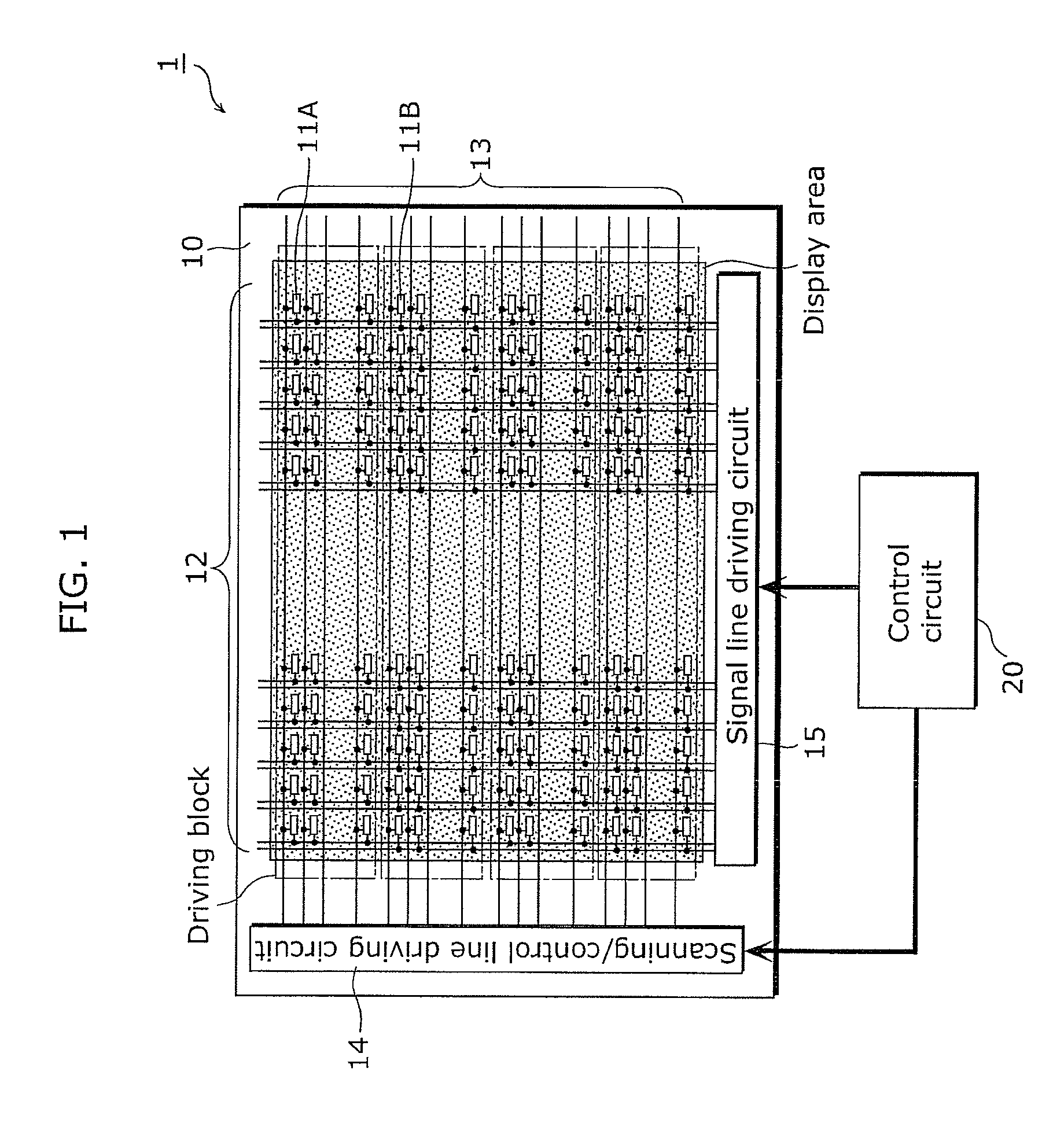
[0048]The image display device according to the present embodiment is an image display device including a plurality of pixels arranged in rows and columns. Each of the pixels includes: a driving transistor which converts a signal voltage which determines luminous intensity into a driving current; a luminescence element which generates photons in response to the driving current flowing through the luminescence element; and a threshold voltage detecting unit configured to detect a threshold voltage of the driving transistor. The pixels make up at least two or more driving blocks each of which includes a plurality of the rows. Furthermore, the image display device further includes a control unit configured to control supply of the reference voltage and a power source voltage to all of the pixels in a same one of the driving blocks with a same timing in a predetermined period to cause all of the threshold voltage detecting units in the same one of the driving blocks to detect the thresh...

second embodiment

[0102]A second embodiment of the present invention will be described below with reference to drawings.

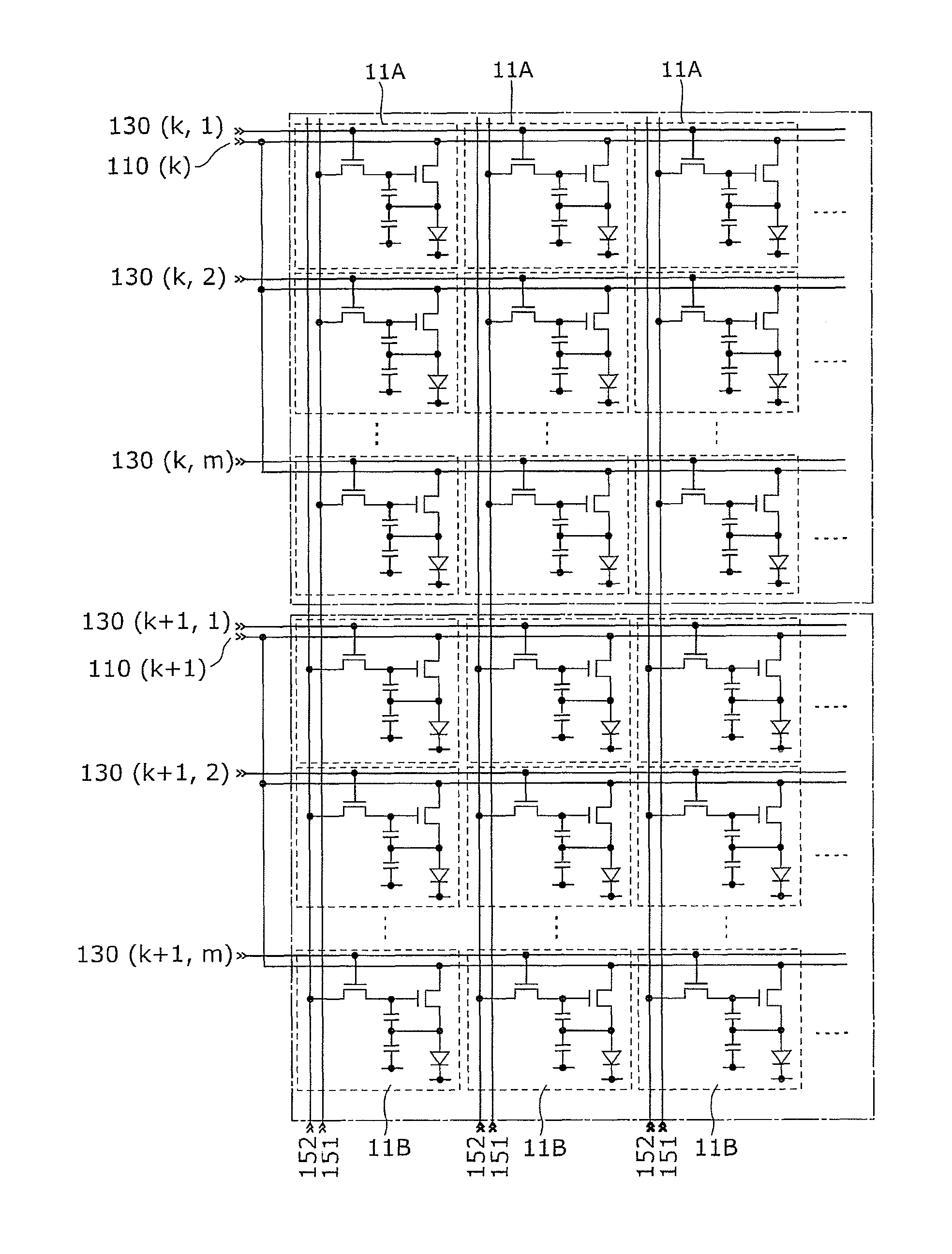
[0103]FIG. 7 is a circuit diagram illustrating a portion of a display panel of an image display device according to the second embodiment of the present invention. Two adjacent driving blocks, scanning liens, and signal lines are depicted in FIG. 7. In FIG. 7, the scanning lines and the signal lines are denoted by “reference numeral (block number, row number in the block) or “reference numeral (block number)”.

[0104]As described earlier, a driving block is made up of a plurality of pixel rows and two or more driving blocks exist in the display panel 10. For example, each driving block depicted in FIG. 7 is made up of m pixel rows.

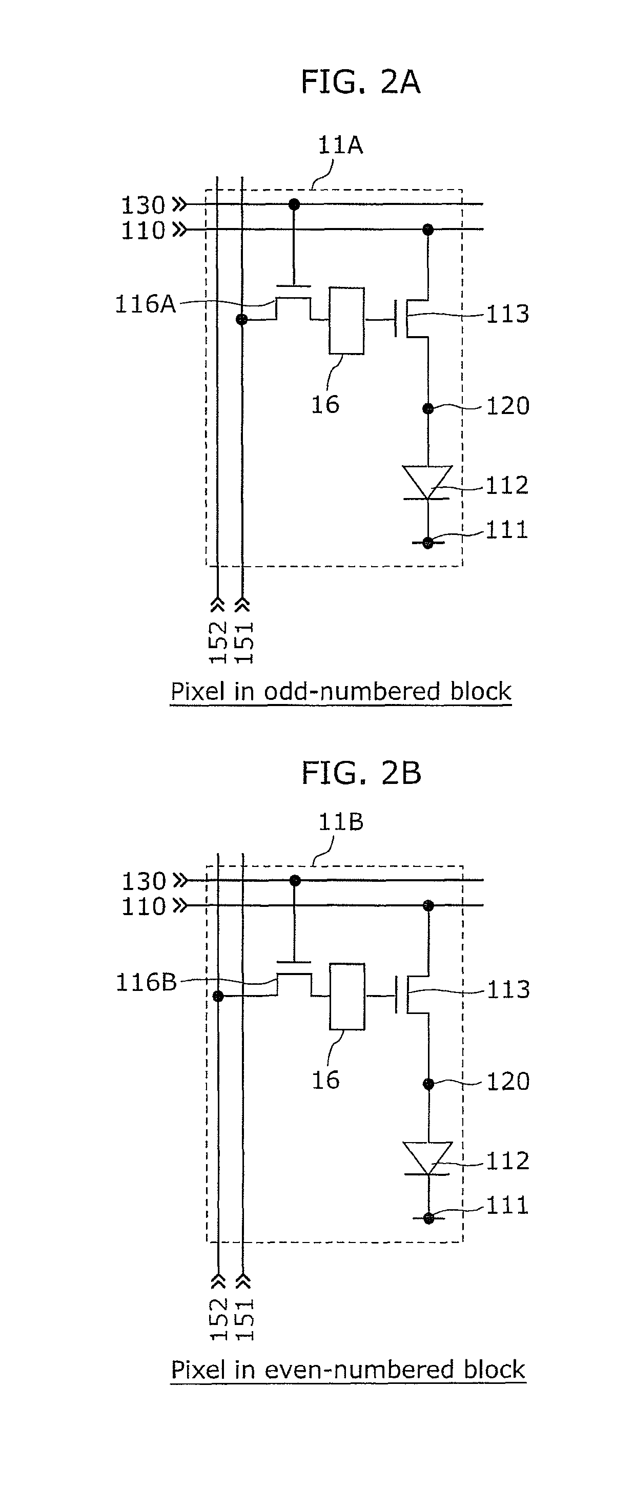
[0105]In the k-th driving block depicted in the upper part of FIG. 7, a power source line 110 (k) is connected to drains of driving transistors 113 of all pixels 11A in common. On the other hand, scanning lines 130 (k, 1) to 130 (k, m) are connected individu...


PUM


Abstract

The image display device includes: a plurality of pixels arranged in a matrix, each of which includes a driving transistor which converts a signal voltage which determines luminous intensity into a driving current; a luminescence element which generates photons according to the driving current flowing through it; and a threshold voltage detecting unit which detects a threshold voltage of the driving transistor while a reference voltage is applied. The pixels make up two or more driving blocks each of which includes a plurality of pixel rows. The image display device controls supply of the reference voltage and a power source voltage to all pixels in the same driving block with the same timing in a predetermined period and controls supply of the reference voltage and the power source voltage to all pixels in different blocks with different timings.

Description

CROSS REFERENCE TO RELATED APPLICATION[0001]This is a continuation application of PCT application No. PCT / JP2010 / 003414 filed on May 21, 2010, designating the United States of America.BACKGROUND OF THE INVENTION[0002](1) Field of the Invention[0003]The present invention relates to image display devices and methods of driving the same and, in particular, to an image display device using current-driven luminescence elements and a method of driving the same.[0004](2) Description of the Related Art[0005]Image display devices using organic electro luminescence (EL) elements are well-known as image display devices using current-driven luminescence elements. An organic EL display device using such organic EL elements which spontaneously generate photons does not require backlights needed in a liquid crystal display, and is therefore ideally suited to achieving reduction of thickness of the devices. In addition, since the organic EL displays have an unrestricted viewing angle, the organic E...

Claims


Application Information

Patent Timeline
Patent Type & Authority Patents(United States)
IPC IPC(8): G09G5/00G09G3/30G06F3/038
CPCG09G3/3233G09G2310/0221G09G2330/021G09G2310/0205G09G2300/0876G09G2320/043G09G2330/028G09G2310/0218G09G2300/0866G09G2320/0626
Inventor ONO, SHINYA
Owner JOLED INC
Why Eureka
Try Eureka