Eureka AIR delivers breakthrough ideas for toughest innovation challenges, trusted by R&D personnel around the world.

Semiconductor manufacturing apparatus

a manufacturing apparatus and semiconductor technology, applied in the field of semiconductor substrate processing, can solve the problems of separation from the stage, and the presence of buffers, so as to prevent breakage or deformation of the semiconductor substrate and improve processing efficiency. the effect of processing efficiency

Active Publication Date: 2014-04-15
MITSUBISHI ELECTRIC CORP
View PDF15 Cites 4 Cited by
  • Summary
  • Abstract
  • Description
  • Claims
  • Application Information

AI Technical Summary

Benefits of technology

[0010]The present invention has been made to solve the problems above, and an object of the invention is to provide a semiconductor manufacturing apparatus capable of preventing breakage and deformation of semiconductor substrates without deteriorating operability in processing.
[0012]According to the semiconductor manufacturing apparatus of the first aspect of the invention, when the semiconductor substrate is placed on the stage, the stress applied to the semiconductor substrate when a contaminant adheres on its back is reduced, and the semiconductor substrate is kept flat. This prevents breakage and deformation of the semiconductor substrate without deteriorating operability in processing.
[0014]According to the semiconductor manufacturing apparatus of the second aspect of the invention, when the semiconductor substrate is placed on the stage, the stress applied to the semiconductor substrate when a contaminant adheres on its back is reduced, and the semiconductor substrate is kept flat. This prevents breakage and deformation of the semiconductor substrate without deteriorating operability in processing.

Problems solved by technology

If the contaminants have certain or higher hardness, the semiconductor substrate undergoes considerable stress at and around the contaminants, which may result in breakage or deformation of the semiconductor substrate.
In the semiconductor manufacturing apparatus disclosed in Patent Document 1, the presence of the buffer, separate from the stage, is likely to deteriorate operability in processing.
Also, in the semiconductor manufacturing apparatuses disclosed in Patent Documents 2 to 4, semiconductor substrates are sucked from the holes, or the like, formed in the surface of the stage Accordingly, when the holes, or the like, are large, the semiconductor substrates undergo considerable stress at and around the holes, which may also result in breakage or deformation of the semiconductor substrates.

Method used


Image

  • Semiconductor manufacturing apparatus
  • Semiconductor manufacturing apparatus
  • Semiconductor manufacturing apparatus

Examples


first preferred embodiment

(First Preferred Embodiment)

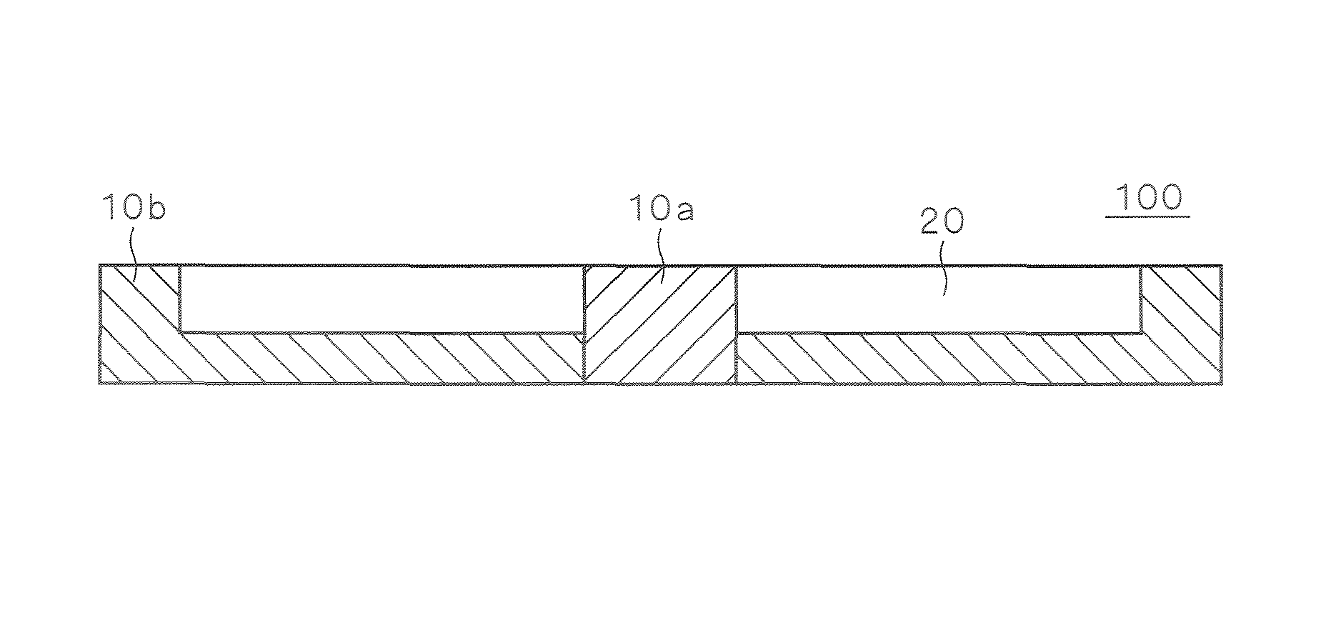
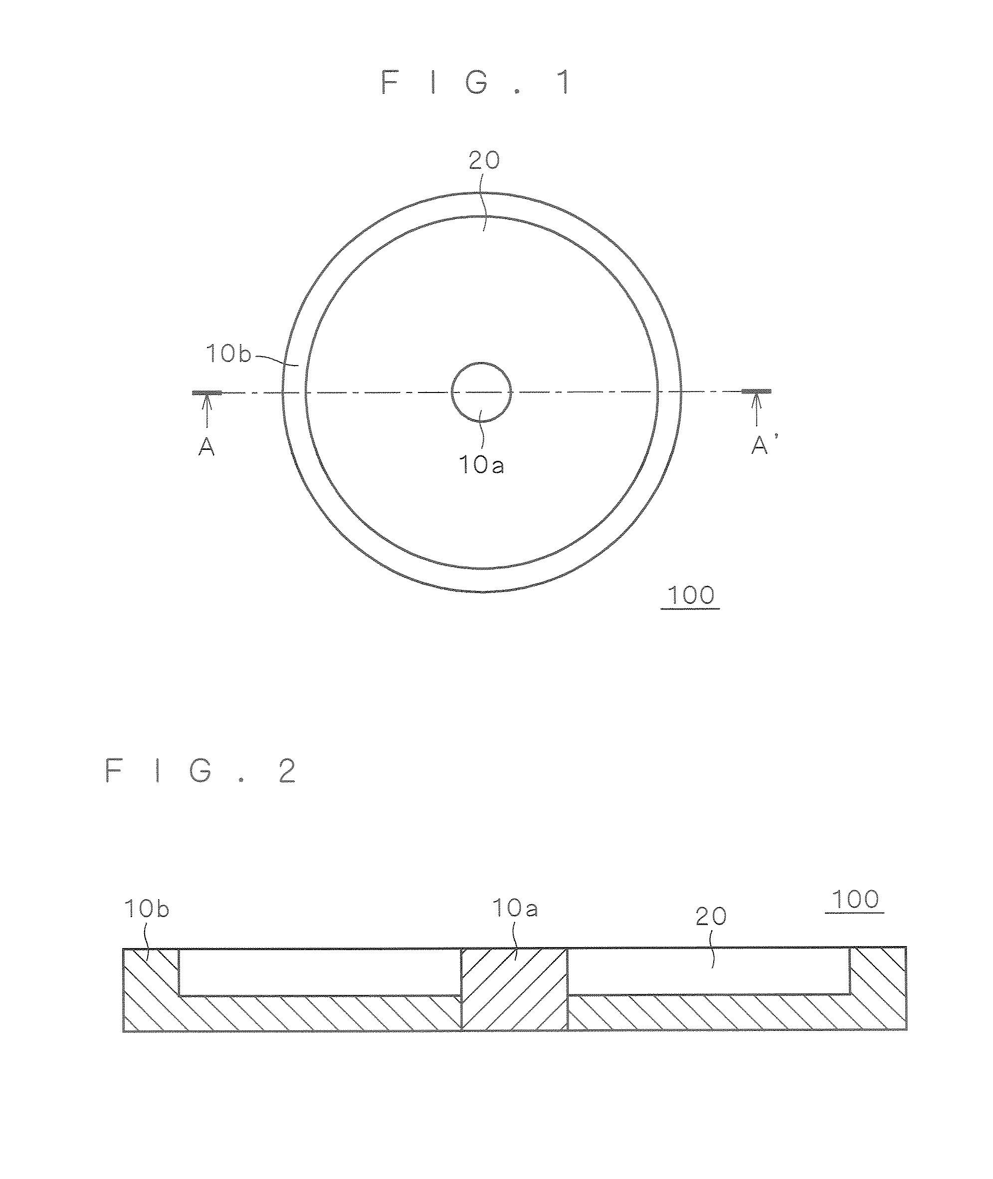
[0039]FIG. 1 is a top view of a stage 100 of a semiconductor manufacturing apparatus according to a first preferred embodiment of the present invention. FIG. 2 shows the cross section taken along line A-A′ of FIG. 1.

[0040]As shown in FIGS. 1 and 2, the stage 100 has metal portions (first metal portion) 10a and 10b that are flat and made of metal, and an electroconductive elastic-body portion 20 that is flat and made of e.g., electroconductive silicone rubber. The metal portions 10a and 10b and the electroconductive elastic-body portion 20 come in close contact with a single semiconductor substrate placed on the stage 100. When the stage 100 is of vacuum suction type, a large number of holes for suction are formed in the metal portions 10a and 10b, which are not shown in FIGS. 1 and 2. The holes may be formed also in the electroconductive elastic-body portion 20.

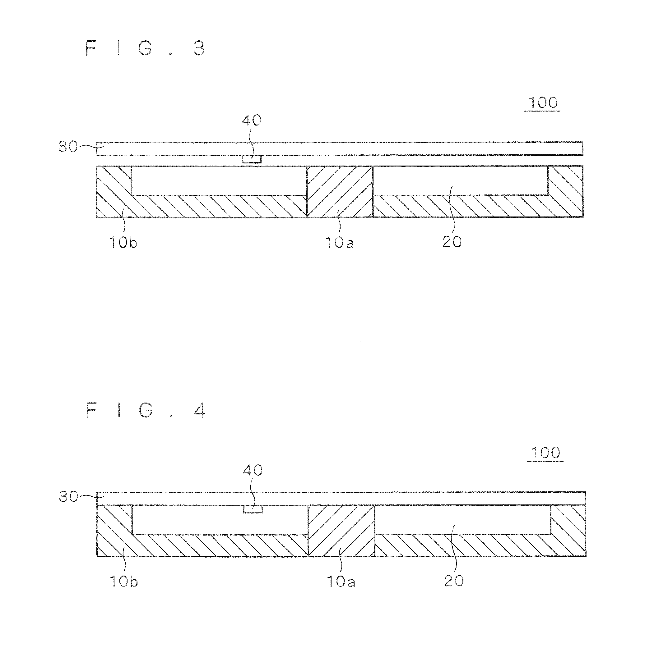
[0041]FIG. 3 is a cross-sectional view showing the stage 100 of FIG. 2 immediately before a sem...

second preferred embodiment

(Second Preferred Embodiment)

[0055]In the stages 100 to 105 of the first preferred embodiment, the flat, electroconductive elastic-body portion 20 of electroconductive silicone rubber is partially formed so that the contaminant 40 is embedded therein to reduce the stress applied to the semiconductor substrate 30. However, a metal portion made of surface-roughened metal may be formed in place of the electroconductive elastic-body portion 20

[0056]FIG. 10 is a top view showing a stage 200 of a semiconductor manufacturing apparatus according to a second preferred embodiment of the present invention. FIG. 11 is an enlarged view showing a part of the cross section taken along line B-B′ of FIG. 10.

[0057]In FIG. 10, the electroconductive elastic-body portion 20 of FIG. 1 is replaced by a metal portion (a second metal portion) 50 that is made of surface-roughened metal. As shown in FIG. 11, the surface of the metal portion 50 has uncounted numbers of recessed portions (recesses) 51 and raise...


PUM

PropertyMeasurementUnit
thicknessaaaaaaaaaa
diameteraaaaaaaaaa
depthaaaaaaaaaa

Abstract

The present invention relates to a semiconductor manufacturing apparatus, and an object of the invention is to prevent breakage and deformation of semiconductor substrates without deteriorating operability in processing.In order to achieve the object, a semiconductor manufacturing apparatus has a stage (100) on which a semiconductor substrate (30) is placed, and the stage (100) has a first metal portion (10) that is made of metal and that comes in contact with the semiconductor substrate (30) placed thereon, and an electroconductive elastic-body portion (20) that is made of an electroconductive elastic body and that comes in contact with the semiconductor substrate (30) placed thereon. A contaminant (40) is embedded in the electroconductive elastic-body portion (20).

Description

TECHNICAL FIELD[0001]The present invention relates to semiconductor manufacturing apparatuses, and particularly to processing of semiconductor substrates.BACKGROUND ART[0002]With vertical semiconductor devices in which current flows between the first and second main surfaces of the semiconductor substrate (semiconductor wafer), the semiconductor substrates are being made thinner and thinner in order to achieve improvements in characteristics (e.g., to reduce on-state voltage). In a common single-wafer-processing semiconductor manufacturing apparatus, the semiconductor substrates are transported to a metal stage having an approximately flat surface and are set on the stage by suction.[0003]Now, thin semiconductor substrates, having a diameter of 6 inches and a thickness of 200 μm or less, for example, have reduced strength Also, when contaminants such as dust and dust particles of Si attach to the back of a semiconductor substrate and the semiconductor substrate is placed on the stag...

Claims


Application Information

Patent Timeline
Patent Type & Authority Patents(United States)
IPC IPC(8): B25B11/00C23C16/00
CPCH01L21/67781H01L21/67769H01L21/68757H01L21/67766H01L21/6875H01L21/67778H01L21/67775H01L21/67772H01L21/67173H01L21/67028H01L21/67757
Inventor TOKUDA, NORIFUMIOKADA, YUUKO
Owner MITSUBISHI ELECTRIC CORP
Why Eureka
Eureka Blog
Learn More