Touch screen panel and display device having the same
a display device and touch screen technology, applied in the field of touch screen panel and display device having the same, can solve the problems of display device visibility degradation and failure of touch screen panel, and achieve the effect of preventing static electricity vulnerability and failure and improving visibility of display panel
- Summary
- Abstract
- Description
- Claims
- Application Information
AI Technical Summary
Benefits of technology
Problems solved by technology
Method used
Image
Examples
first embodiment
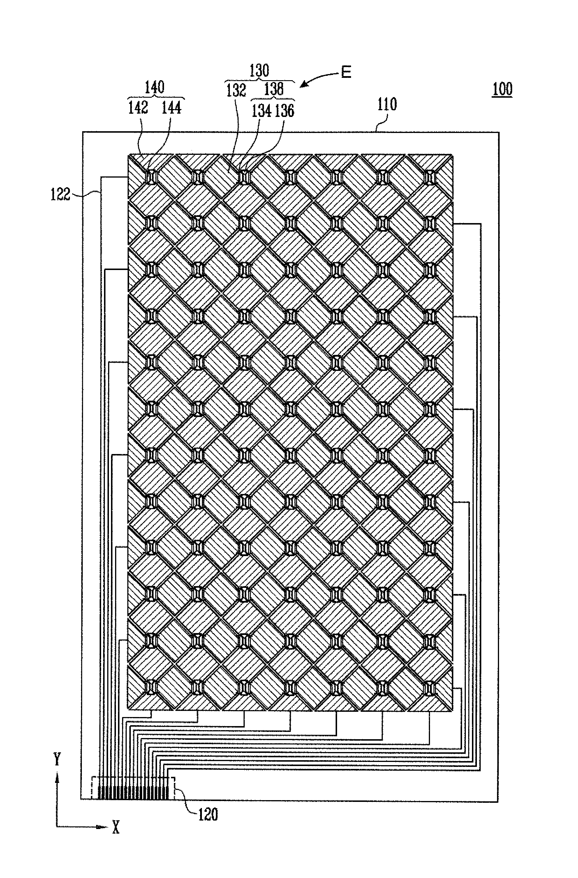
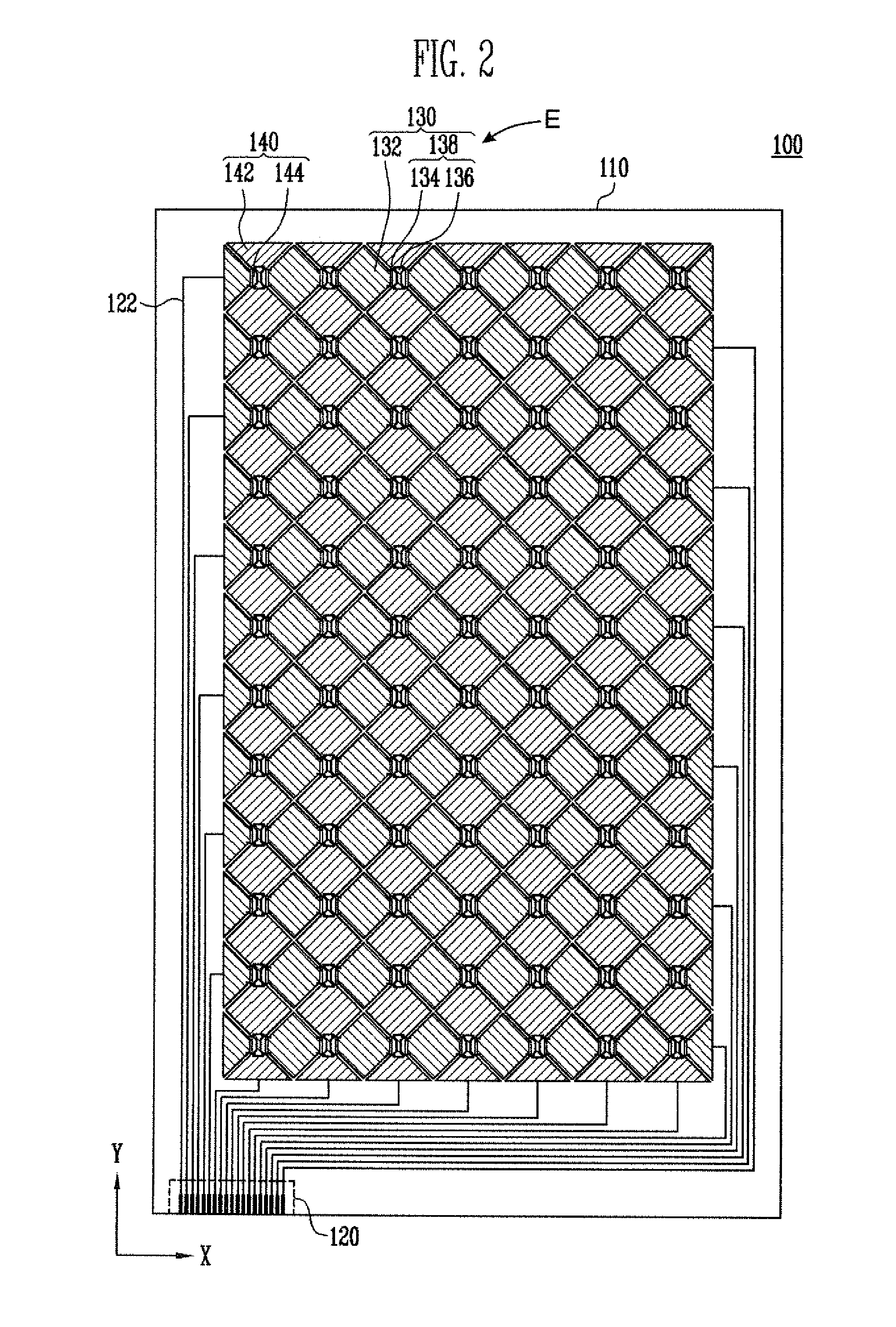
[0036]FIG. 2 is a plan view showing a touch screen panel according to the present invention; and FIG. 3 is a main part enlarged view showing an embodiment of sensing cells and connection patterns at portion E shown in FIG. 2.
[0037]Referring to FIGS. 2 and 3, a touch screen panel 100 according to a first embodiment of the present invention includes a transparent substrate 110, sensing patterns 130 and 140 formed in an active area on the transparent substrate 110, and position detecting lines 122 formed in a non-active area outside the active area.
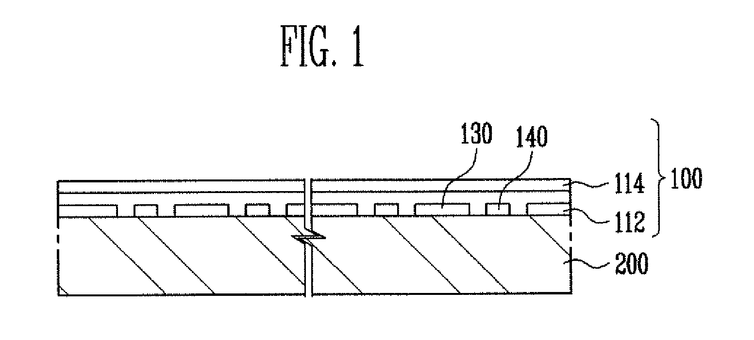
[0038]The transparent substrate 110 may be an upper substrate which constitutes the display panel 200 of FIG. 1 in the display device. Alternatively, the transparent substrate 110 may be a separate substrate attached to the display panel 200.
[0039]The sensing patterns 130 and 140 are alternately arranged, and include first sensing patterns 130 formed so as to be connected to one another for each row having the same X coordinate, and second s...
second embodiment
[0073]FIG. 5 is a plan view showing a touch screen panel according to the present invention; and FIG. 6 is a main part enlarged view showing an embodiment of sensing cells and connection patterns at portion E shown in FIG. 5.
[0074]Referring to FIGS. 5 and 6, the touch screen panel 100 according to a second embodiment of the present invention includes a transparent substrate 210, sensing patterns 230 and 240 formed in an active area on the transparent substrate 210, and position detecting lines 222 formed in a non-active area at the outside of the active area. Since the position detecting lines 222 and a pad portion 220 are identical to those described in the first embodiment, their descriptions will be omitted.
[0075]The transparent substrate 210 may be an upper substrate which constitutes the display panel 200 in the display device. Alternatively, the transparent substrate 210 may be a separate substrate attached to the display panel 200.
[0076]The sensing patterns 230 and 240 are al...
PUM
 Abstract
Description
Claims
Application Information


