Check patentability & draft patents in minutes with Patsnap Eureka AI!

Photo element and driving method thereof and liquid crystal display

a technology of photo elements and liquid crystal displays, applied in the field of liquid crystal displays, can solve the problems of reducing the signal to noise ratio (s/n), incorrect point of touch event determination, and important reliability of photo elements b>100/b> after a long-term illumination

Active Publication Date: 2014-04-22
HANNSTAR DISPLAY CORPORATION
View PDF4 Cites 1 Cited by
  • Summary
  • Abstract
  • Description
  • Claims
  • Application Information

AI Technical Summary

Problems solved by technology

The worse decay of the photo-induced current reduces the signal to noise (S / N) ratio and may result in incorrect point of touch event to be determined.
Hence, the reliability of the photo element 100 after a long-term illumination is an important issue.
By contrast, as shown in FIG. 4, when a voltage, for example, 6V, is stressed to the gate of the photo thin-film transistor for 231 hours, the photo-induced current is decayed about 45.28%; therefore the reliability is unacceptable when the photo element is operated at 1500 lux.

Method used


Image

  • Photo element and driving method thereof and liquid crystal display
  • Photo element and driving method thereof and liquid crystal display
  • Photo element and driving method thereof and liquid crystal display

Examples


Embodiment Construction

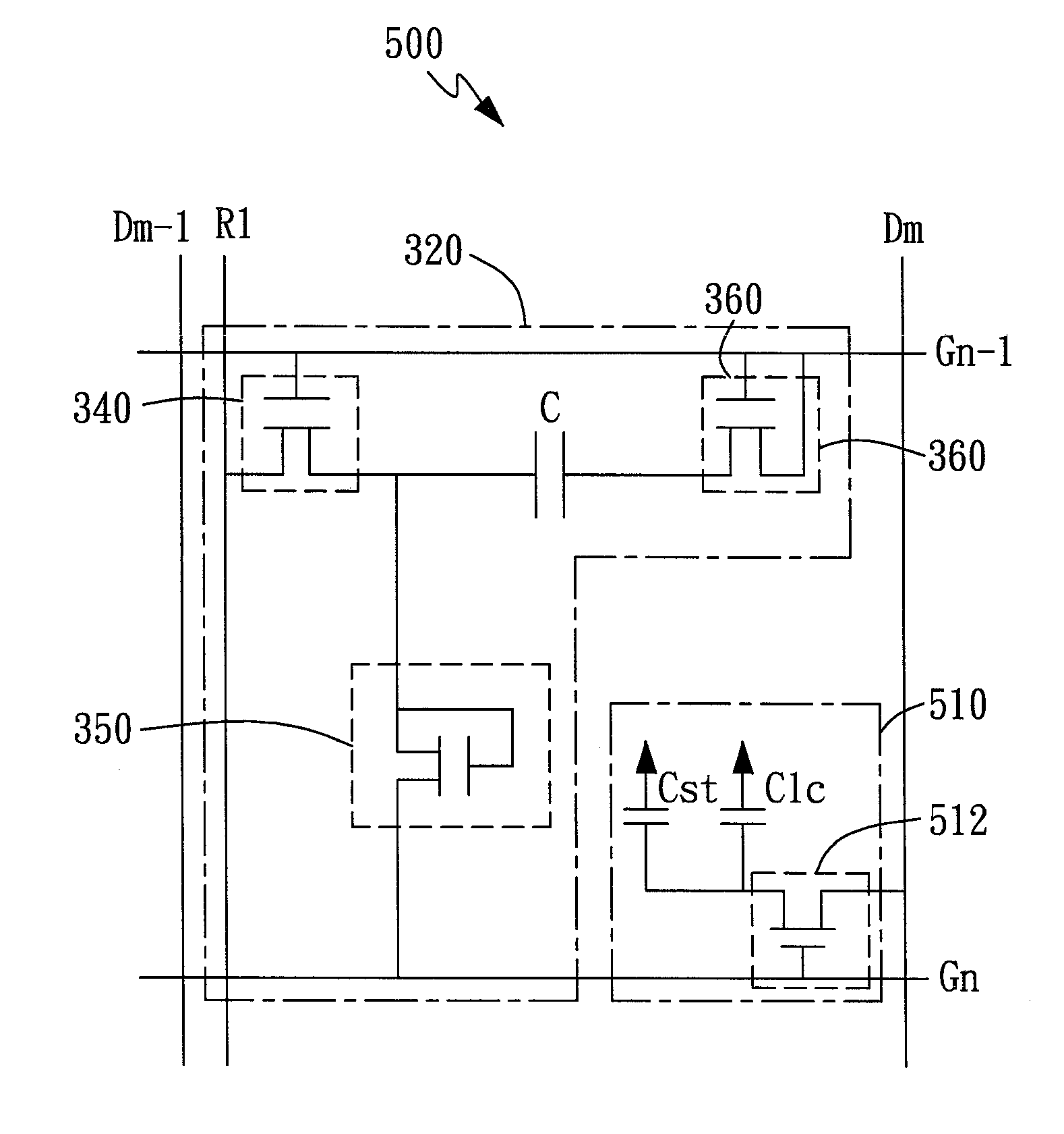
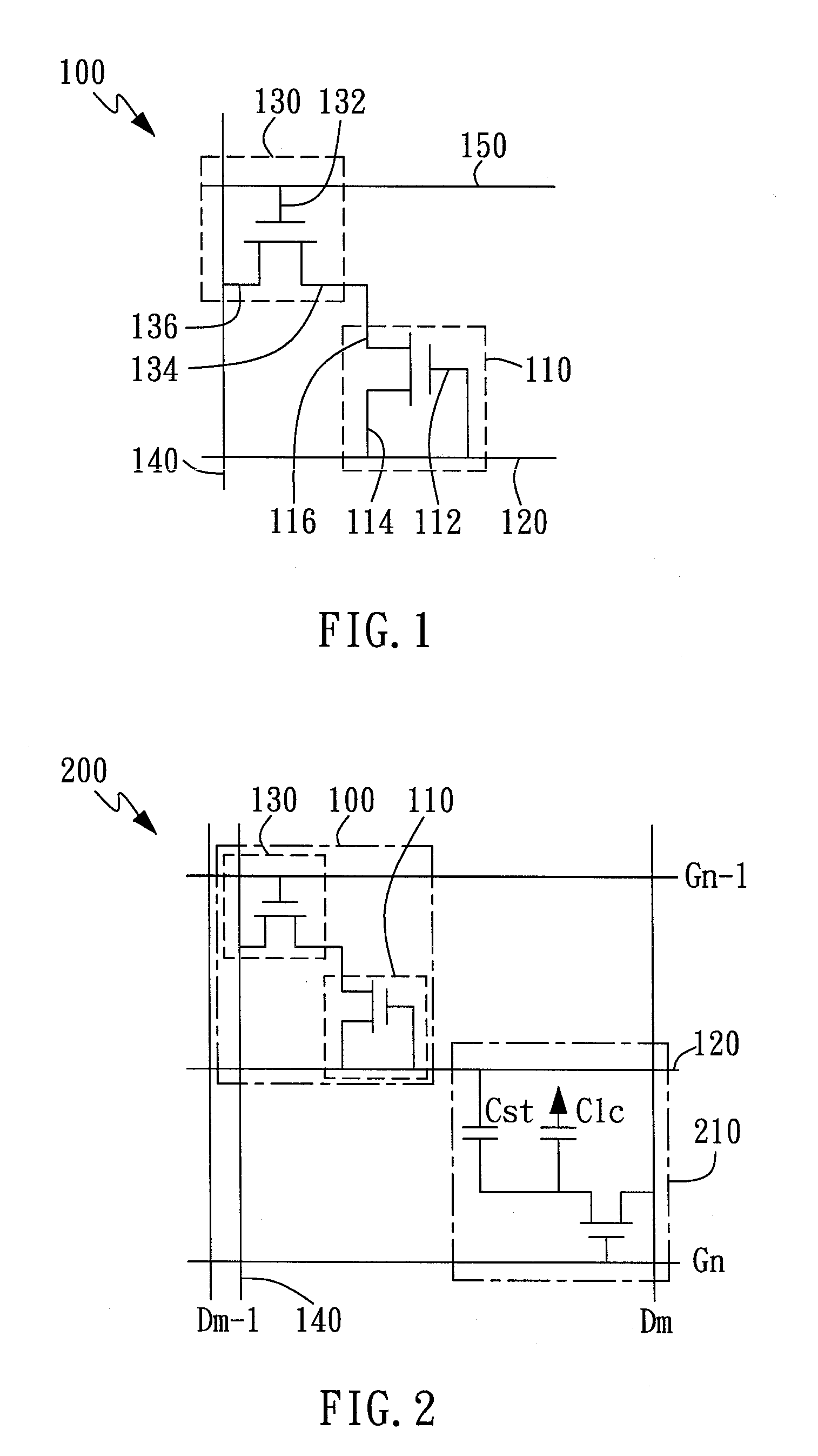
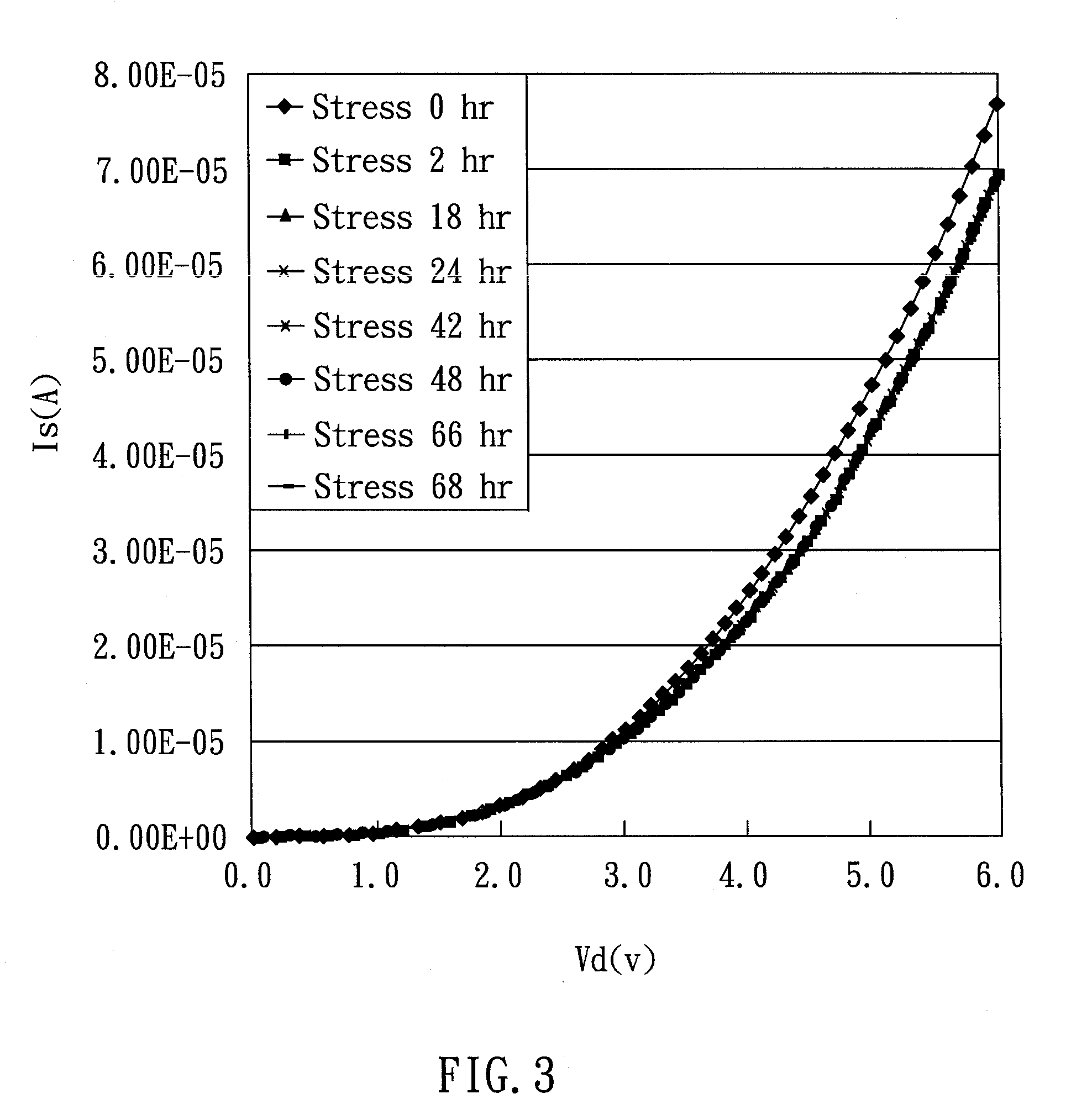
[0024]Reference will now be made in detail to specific embodiments of the invention. Examples of these embodiments are illustrated in accompanying drawings. While the invention will be described in conjunction with these specific embodiments, it will be understood that it is not intended to limit the invention to these embodiments. On the contrary, it is intended to cover alternatives, modifications, and equivalents as may be included within the spirit and scope of the invention as defined by the appended claims. In the following description, numerous specific details are set forth in order to provide a through understanding of the present invention. The present invention may be practiced without some or all of these specific details. In other instances, well-known components and process operations are not described in detail in order not to unnecessarily obscure the present invention. While drawings are illustrated in details, it is appreciated that the quantity of the disclosed co...


PUM


Abstract

A photo element includes a capacitor, a switch thin film transistor (TFT), a charge thin film transistor, and a photo thin film transistor. A voltage is charged to the capacitor through the charge TFT, and the output voltage of the capacitor is read through the readout line. The photo-induced current will affect the output voltage of the capacitor; therefore it is employed to determine whether the photo element is touched. Later, a reverse-biased voltage is applied to the photo TFT, such that the threshold voltage and sensitivity of the photo TFT can be maintained.

Description

BACKGROUND OF THE INVENTION[0001]1. Field of the Invention[0002]The present invention relates to a Liquid Crystal Display, and more particularly, to a Liquid Crystal Display with in-cell touch panel.[0003]2. Description of the Prior Art[0004]One type of touch panel, “In-cell touch panel,” comprises many photo elements capable of sensing the light and thus inducing photo-induced currents. By sensing the variance of the photo-induced current, the coordinates of the user's touched points can be determined.[0005]FIG. 1 shows a conventional photo element 100 of an In-cell touch panel. The photo element 100 comprises a photo thin-film transistor 110 and a switch thin-film transistor 130. The source 136 of the switch thin-film transistor 130 is connected to a readout line 140; the gate 132 of the switch thin-film transistor 130 is connected to a switch line 150; the drain 134 of the switch thin-film transistor 130 is connected to the source of the photo thin-film transistor 110. Further, T...

Claims


Application Information

Patent Timeline
Patent Type & Authority Patents(United States)
IPC IPC(8): G06F3/042
CPCG06F3/0412G02F1/13338G06F3/042G02F2001/13312G02F1/13312
Inventor CHANG, HUNG-CHANGJUAN, YI-CHUNGWU, CHAO-HUI
Owner HANNSTAR DISPLAY CORPORATION
Features
  • R&D
  • Intellectual Property
  • Life Sciences
  • Materials
  • Tech Scout
  • Unparalleled Data Quality
  • Higher Quality Content
  • 60% Fewer Hallucinations
Learn More