Solid-state imaging apparatus

a solid-state imaging and apparatus technology, applied in the field of solid-state imaging apparatus, can solve the problems of aggravating the linearity of a/d conversion and achieve the effect of enhancing the accuracy of a/d conversion

Active Publication Date: 2014-04-29
CANON KK
View PDF54 Cites 39 Cited by
  • Summary
  • Abstract
  • Description
  • Claims
  • Application Information

AI Technical Summary

Problems solved by technology

However, when the capacitive feedback type amplifier is used in the ramp signal generating circuit, there has been a problem that because the capacitance of the capacitor element has voltage dependency, the linearity in the A / D conversion results in being aggravated.

Method used


Image

  • Solid-state imaging apparatus
  • Solid-state imaging apparatus
  • Solid-state imaging apparatus

Examples


first embodiment

[0020]A first embodiment of the disclosure will be described below.

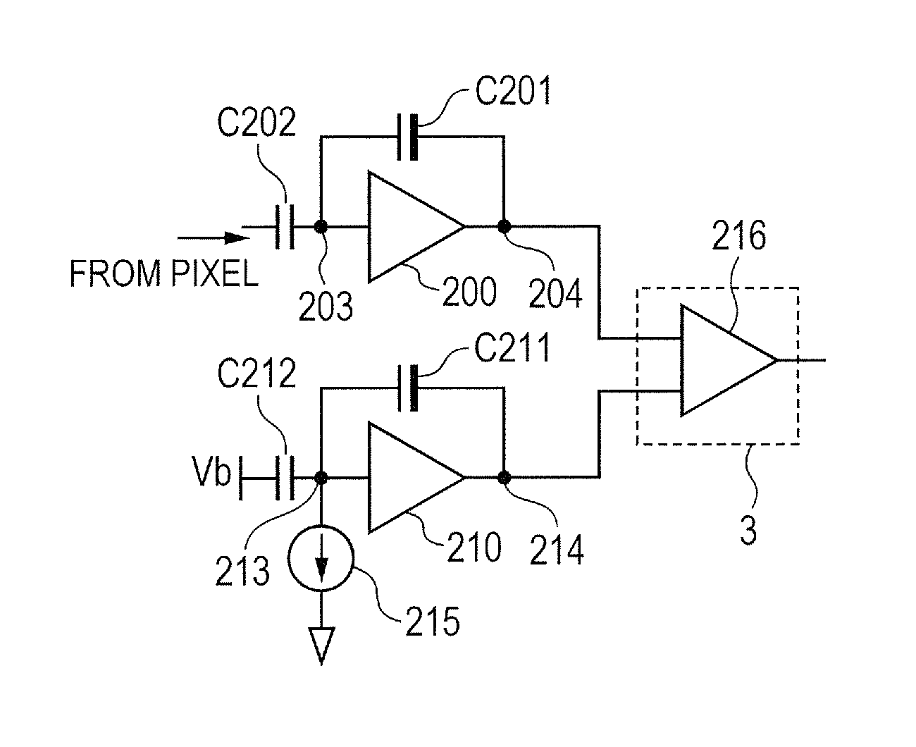
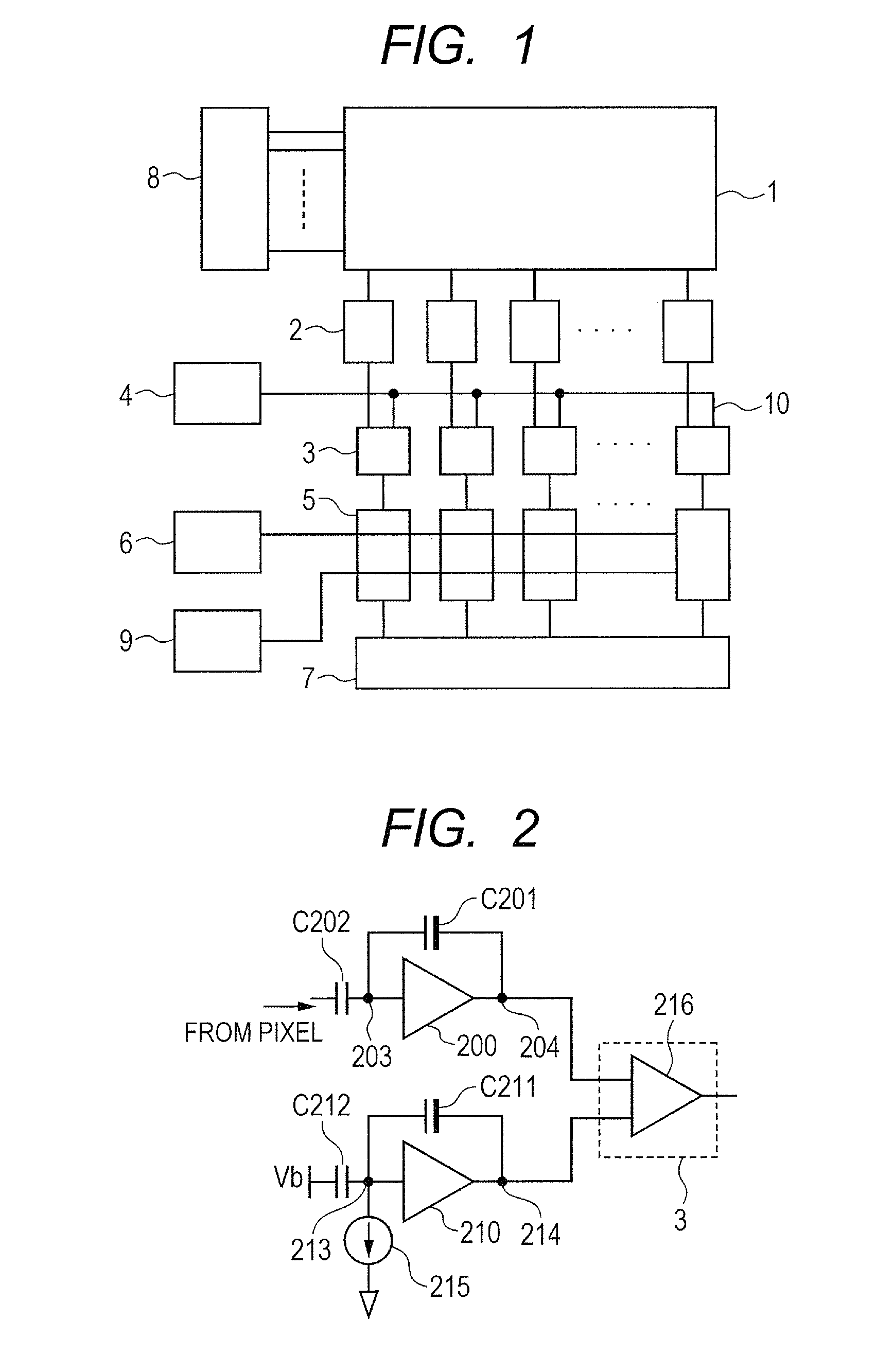
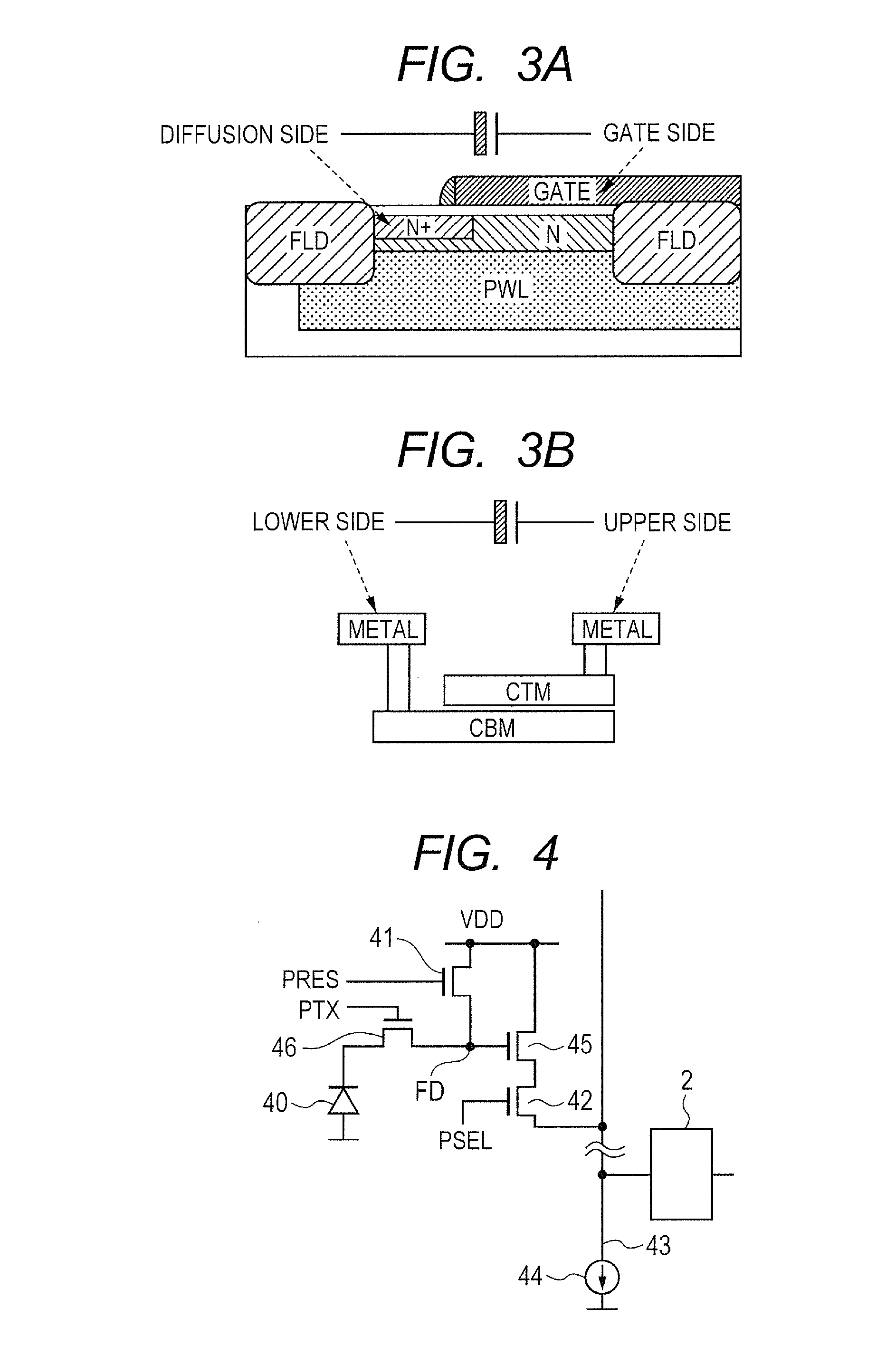
[0021]FIG. 1 is a schematic view illustrating a configuration example of a circuit of a solid-state imaging apparatus according to a first embodiment. The solid-state imaging apparatus has a pixel unit 1, an amplifier circuit 2, a comparison unit 3, a reference signal generating circuit 4, a storage unit 5, a counter circuit 6, a horizontal scanning circuit 7, a vertical scanning circuit 8 and a signal processing circuit 9. The pixel unit 1 has a plurality of pixels including a photoelectric conversion element, and the pixels are arranged two dimensionally in the unit (line direction and column direction). The amplifier circuit 2, the comparison unit 3 and the storage unit 5 are arranged in each of the columns so as to correspond to each of the columns of the pixel unit 1. The comparison unit 3, the storage unit 5 and the counter circuit 6 constitute an A / D conversion circuit for analog-to-digital converting the pixe...

second embodiment

[0044]Next, the second embodiment of the disclosure will be described below.

[0045]The solid-state imaging apparatus according to the second embodiment is similar to the above described solid-state imaging apparatus according to the first embodiment except for the reference signal generating circuit, and accordingly a part which is different from the first embodiment will be described below. FIGS. 6A to 6C are views illustrating a configuration example of a circuit of a reference signal generating circuit 4 according to the second embodiment.

[0046]As is illustrated in FIG. 6A, the reference signal generating circuit 4 has a computing amplifier 60, a feedback capacitor C61, a low pass filter including an input capacitor C62 and an input resistance R63, and a signal generating unit 66. The computing amplifier 60 is a reversal amplifier, and the input terminal 64 is connected to the signal generating unit 66 through a series circuit in which the input capacitor C62 and the input resista...


PUM


Abstract

A solid-state imaging apparatus includes: an amplifier circuit configured to amplify a signal from pixel; and a reference signal generating circuit configured to generate a ramp signal, wherein feedback capacitor elements having the same structure are electrically connected to a capacitive feedback type amplifier of the amplifier circuit and to a capacitive feedback type amplifier of the reference signal generating circuit respectively, and a connecting configuration between an amplifier of the amplifier circuit and the feedback capacitor element and a connecting configuration between an amplifier of the reference signal generating circuit and the feedback capacitor element are the same.

Description

BACKGROUND OF THE INVENTION[0001]1. Field of the Invention[0002]One disclosed aspect of the embodiments relates to a solid-state imaging apparatus having an analog-to-digital conversion circuit (A / D conversion circuit).[0003]2. Description of the Related Art[0004]A solid-state imaging apparatus such as a CMOS image sensor, which has an A / D conversion circuit built-in, is used in an image-inputting equipment such as a digital camera. The A / D conversion circuit which is built in the solid-state imaging apparatus obtains digital data by subjecting a pixel signal in each column and a ramp signal (reference signal) which is common in each column, to comparison processing. Japanese Patent Application Laid-Open No. 2008-187420 discloses a structure of obtaining the ramp signal by charging and discharging an electric current to / from a capacitive feedback type amplifier, for a ramp signal generating circuit for generating a ramp signal.SUMMARY OF THE INVENTION[0005]However, when the capaciti...

Claims


Application Information

Patent Timeline
Patent Type & Authority Patents(United States)
IPC IPC(8): H03K5/153H04N9/83H04N3/14H04N9/083
CPCH03F2200/78H03F2203/45512H03F2203/45544H03F3/45475
Inventor MAEHASHI, YUHIYAMA, HIROKIITANO, TETSUYASAITO, KAZUHIRONAKAMURA, KOHICHI
Owner CANON KK
Why Eureka
Try Eureka