Light emitting diode package having a portion of reflection cup material covering electrode layer on side surfaces of substrate

a technology of light-emitting diodes and reflection cups, which is applied in the direction of semiconductor/solid-state device manufacturing, electrical equipment, semiconductor devices, etc., can solve the problem of depressed luminous efficiency of led packages

Inactive Publication Date: 2014-05-06
ADVANCED OPTOELECTRONIC TECH INC
View PDF9 Cites 2 Cited by
  • Summary
  • Abstract
  • Description
  • Claims
  • Application Information

AI Technical Summary

Benefits of technology

[0004]In recent years, light emitting diodes (LEDs) have become more and more popular, due to their low power-consumption, energy saving properties, high efficiency, short reactive time and long life. A typical LED package includes a sapphire substrate on which a reflection cup is formed, and a light-emitting chip placed in the reflection cup and attached on the sapphire substrate. However, a gap exists between the substrate and the reflection cup, such that vapor and dust tend to intrude the LED package, the light-emitting chip would be influenced thereby, and the luminous efficiency of the LED package may be depressed.

Problems solved by technology

However, a gap exists between the substrate and the reflection cup, such that vapor and dust tend to intrude the LED package, the light-emitting chip would be influenced thereby, and the luminous efficiency of the LED package may be depressed.

Method used


Image

  • Light emitting diode package having a portion of reflection cup material covering electrode layer on side surfaces of substrate
  • Light emitting diode package having a portion of reflection cup material covering electrode layer on side surfaces of substrate
  • Light emitting diode package having a portion of reflection cup material covering electrode layer on side surfaces of substrate

Examples


Embodiment Construction

[0009]Reference will now be made to the drawings to describe the present LED package and method for manufacturing the same in detail.

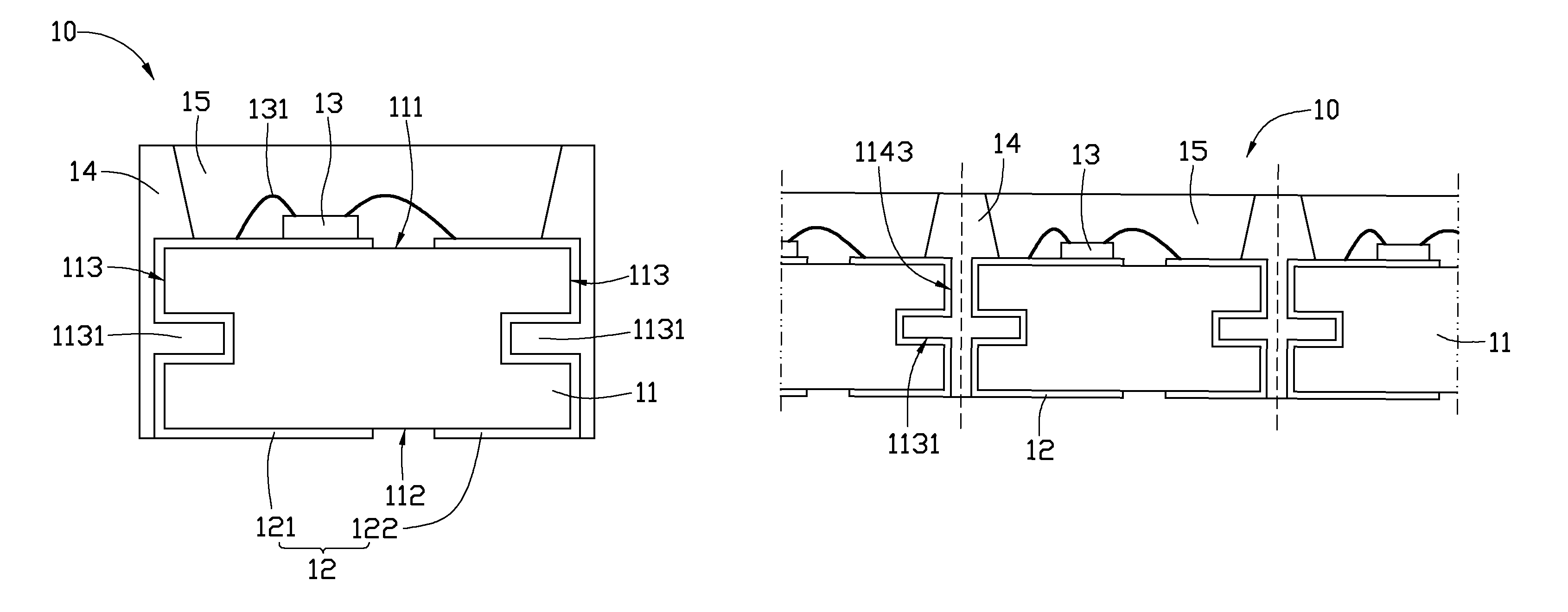
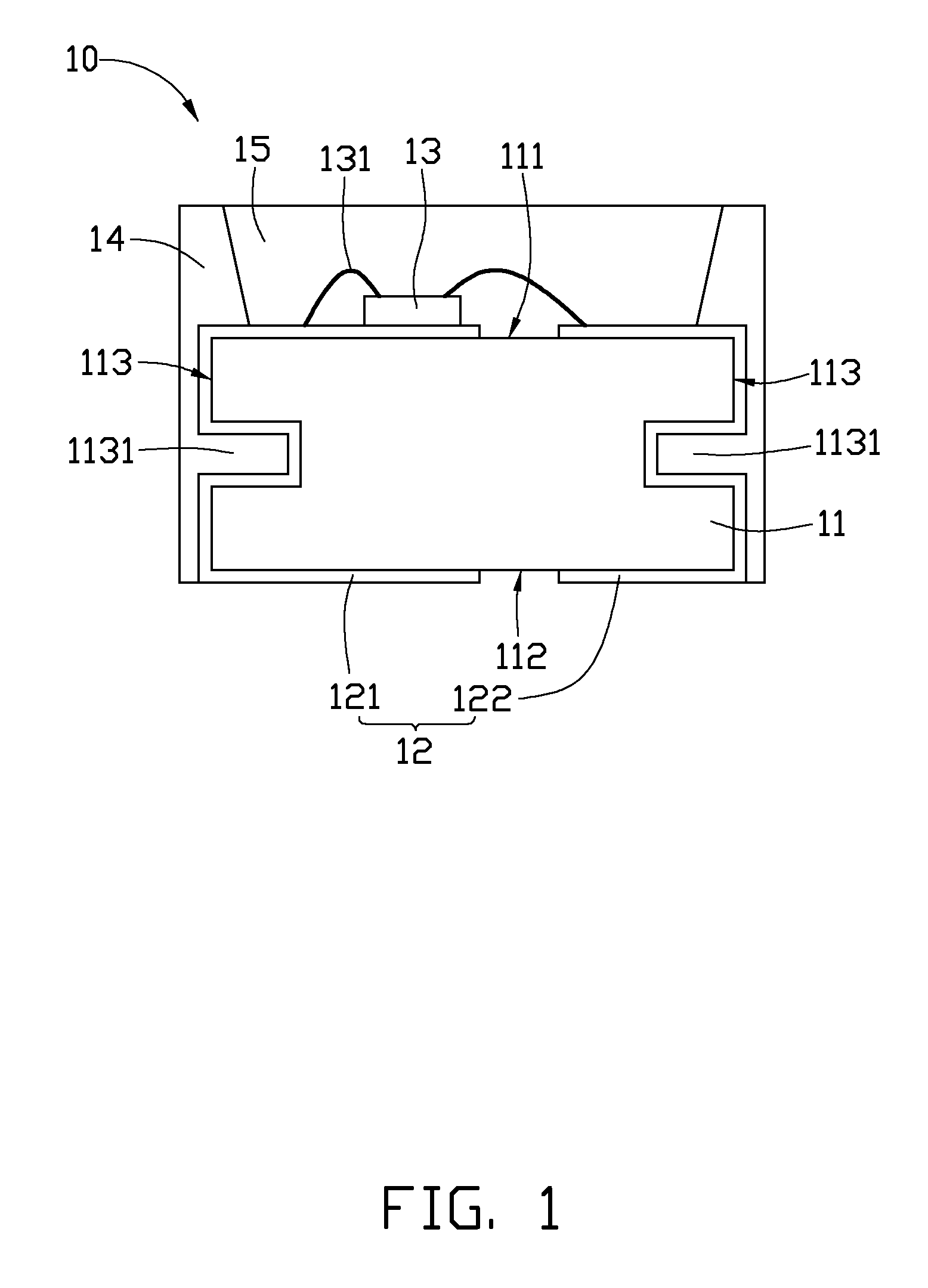
[0010]Referring to FIG. 1, an LED package 10 according to an exemplary embodiment includes a substrate 11, an electrode layer 12, a light-emitting chip 13, a reflection cup 14, and an encapsulation 15.

[0011]The substrate 11 includes a first surface 111 (i.e., top surface), an opposite second surface 112 (i.e., bottom surface), and two side surfaces 113 connected between left and right edges of the first surface 111 and the second surface 112, respectively. The side surfaces 113 each have a recess 1131 defined therein. An extending (recessed) direction of the recess 1131 is parallel to the first surface 111. The recesses 1131 can be shaped with any configuration according to a computer simulation in advance. Alternatively, the recesses 1131 respectively defined on the two side surfaces 113 can be further recessed to communicate with each other.
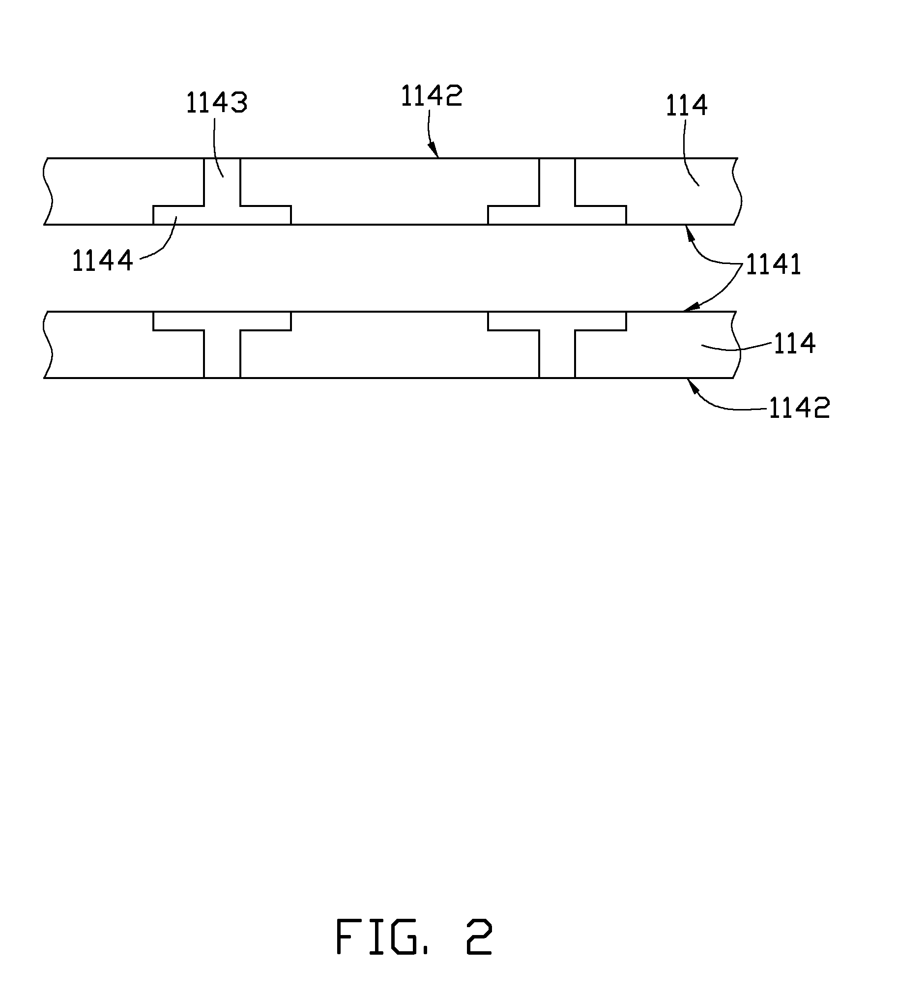
[0012]The...


PUM


Abstract

An LED package includes a substrate, an electrode layer, a light-emitting chip, a reflection cup and an encapsulation. The substrate includes a first surface, an opposite second surface, and two side surfaces. The electrode layer is consisted of a positive electrode and a negative electrode, each of which extends from the first surface to the second surface via a respective side surface. The light-emitting chip is located on the first surface of the substrate and electrically connected to the electrode layer. The reflection cup comprises a first part covering the electrode layer on the side surfaces of the substrate, a second part with a bowl-like shape on the first surface of the substrate and surrounding the light-emitting chip. The encapsulation is filled in the second part of the reflection cup.

Description

BACKGROUND[0001]1. Technical Field[0002]The present disclosure generally relates to light emitting diode (LED) packages and method of manufacturing the same.[0003]2. Description of Related Art[0004]In recent years, light emitting diodes (LEDs) have become more and more popular, due to their low power-consumption, energy saving properties, high efficiency, short reactive time and long life. A typical LED package includes a sapphire substrate on which a reflection cup is formed, and a light-emitting chip placed in the reflection cup and attached on the sapphire substrate. However, a gap exists between the substrate and the reflection cup, such that vapor and dust tend to intrude the LED package, the light-emitting chip would be influenced thereby, and the luminous efficiency of the LED package may be depressed.[0005]Therefore, it is necessary to provide an LED package and a method of manufacturing the same which can overcome the above shortcomings.BRIEF DESCRIPTION OF THE DRAWINGS[000...

Claims


Application Information

Patent Timeline
Patent Type & Authority Patents(United States)
IPC IPC(8): H01L33/48H01L33/38
CPCH01L24/97H01L33/486H01L2924/01029H01L33/62H01L2924/12041H01L2933/0033H01L33/385H01L2924/10253H01L2224/48227H01L33/60H01L2224/48091H01L2924/00014H01L2924/00
Inventor TSAI, MING-TACHEN, CHING-CHUNG
Owner ADVANCED OPTOELECTRONIC TECH INC
Why Eureka
Try Eureka