Border between semiconductor transistors with different gate structures

a technology of semiconductor transistors and gate structures, which is applied in the direction of semiconductor devices, electrical equipment, transistors, etc., can solve the problems of occurrence of depletion of gate electrodes, relative increase in the strength of electric field on the gate electrodes, and short circuit lines, so as to prevent short circuits

Active Publication Date: 2014-06-03
LONGITUDE LICENSING LTD
View PDF4 Cites 0 Cited by
  • Summary
  • Abstract
  • Description
  • Claims
  • Application Information

AI Technical Summary

Benefits of technology

[0024]According to the invention, the border between the first region, in which a first transistor that has a HKMG structure is formed, and the second region, in which a second transistor that has a HKMG structure is formed, the layered structure of electrode materials of which is different from that of the first transistor, overlaps with at most only the first line or the second line that are of different potentials. Accordingly, even if some residue is generated on the border between the first region and the second region, a short circuit can be prevented from occurring between the first line and the second line.

Problems solved by technology

One problem of a thinner gate insulating film is the relative increase in the strength of the electric field on the gate electrode, and is occurrence of depletion of the gate electrode composed of polysilicon.
Another problem of a thinner gate insulating film is occurrence of the so-called tunnel current caused by electrons, which would flow through a channel, tunneling a bather formed by the silicon oxide film so as to flow through the gate electrode.
The present inventor has now discovered a problem in which a residue of a GS layer is generated during the gate processing and the residue may cause short circuit lines.

Method used


Image

  • Border between semiconductor transistors with different gate structures
  • Border between semiconductor transistors with different gate structures
  • Border between semiconductor transistors with different gate structures

Examples


Embodiment Construction

[0045]The invention will be now described herein with reference to illustrative embodiments. Those skilled in the art will recognize that many alternative embodiments can be accomplished using the teachings of the present invention and that the invention is not limited to the embodiments illustrated for explanatory purposes.

[0046]Exemplary embodiments will now be described with reference to the drawings.

[0047]First, the mechanism of how residue, as described above, is generated will now be described in detail with reference to FIGS. 1 to 7. In FIGS. 1 to 7, same reference numerals represent same components, and the description will be omitted.

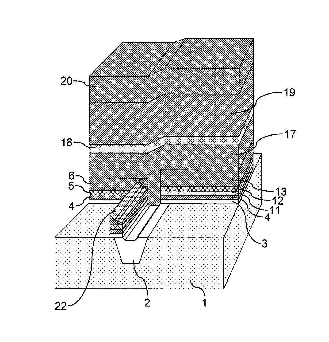
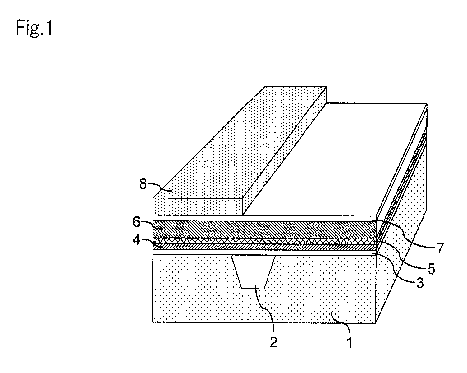
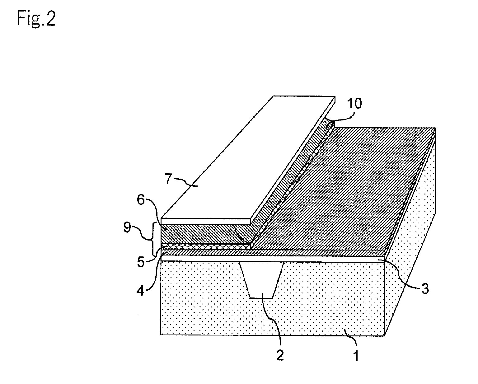
[0048]As shown in FIG. 1, a device isolation region, i.e. shallow trench isolation (STI) 2, is formed on Si substrate 1, which is a semiconductor substrate.

[0049]After STI 2 is formed, silicon oxide (SiO2) film 3 is formed by thermal oxidation as an interlayer. After silicon oxide film 3 is formed, high-k insulating film 4 is deposited, which i...


PUM


Abstract

A semiconductor device according to the invention includes: a first region on a semiconductor substrate, in which a first transistor is formed, the first transistor including first gate insulating film 4 containing a high dielectric constant material and first metal gate electrode 5 formed on first gate insulating film 4; a second region adjacent to the first region on the semiconductor substrate, in which a second transistor is formed, the second transistor including second gate insulating film 4 and second metal gate electrode 12 formed on the second gate insulating film, a layered structure of electrode materials of the second transistor being different from a layered structure of electrode materials of the first transistor; and a first and a second line, the lines being of different potentials, wherein a border between the first and the second region overlaps with at most only the first or the second line.

Description

BACKGROUND OF THE INVENTION[0001]1. Field of the Invention[0002]The present invention relates to a semiconductor device including a transistor that has a HKMG structure.[0003]2. Description of the Related Art[0004]In a metal-insulator-semiconductor field-effect transistor (MISFET) that has a gate insulating film and a gate electrode formed on the gate insulating film, it has been a common practice to use a silicon oxide film, SiO2 in this case, as the gate insulating film and a polysilicon film as the gate electrode.[0005]Recently, the thickness of gate insulating film has been further reduced with miniaturization of MISFETs. One problem of a thinner gate insulating film is the relative increase in the strength of the electric field on the gate electrode, and is occurrence of depletion of the gate electrode composed of polysilicon. Another problem of a thinner gate insulating film is occurrence of the so-called tunnel current caused by electrons, which would flow through a channel, ...

Claims


Application Information

Patent Timeline
Patent Type & Authority Patents(United States)
IPC IPC(8): H01L21/70
CPCH01L27/092H01L21/823842H01L27/105H01L27/0207H01L21/82345H01L27/1052H10B99/00
Inventor KISHIDA, TAKESHI
Owner LONGITUDE LICENSING LTD
Why Eureka
Try Eureka