Semiconductor device

a technology of semiconductor devices and gate electrodes, applied in semiconductor devices, semiconductor/solid-state device details, electrical apparatus, etc., can solve the problems of difficult control of the amount of siliciding formed by the minute gate electrode, the dimension of the gate electrode and the distance between adjacent ones of the gate electrodes is reduced, and the short circuit between the gate electrode and the dummy gate electrode is prevented, so as to achieve high yield and prevent short circuit

Active Publication Date: 2009-02-24
GK BRIDGE 1
View PDF6 Cites 0 Cited by
  • Summary
  • Abstract
  • Description
  • Claims
  • Application Information

AI Technical Summary

Benefits of technology

[0009]In a semiconductor device including dummy gate electrodes as described above and utilizing a silicidation technique, a gate electrode necessary for circuit operation may be formed adjacent to a dummy gate electrode that is unnecessary for circuit operation. The respective upper parts of the gate electrode and the dummy gate electrode are both silicided. Since this silicidation increases the volume of polysilicon used as a material of the gate electrode, the respective upper parts of the gate electrode and the dummy gate electrode are expanded. Therefore, it is likely to cause a short circuit between the gate electrode and the dummy gate electrode. When the gate electrode is electrically connected to the dummy gate electrode, this is very likely to cause a problem in the operation of the semiconductor device due to the low resistance of silicide at which the gate electrode is connected to the dummy gate electrode and other reasons. In addition, the dimensions of gate electrodes and the distance between adjacent ones of gate electrodes are reduced with each passing year, and it is difficult to control the amount of silicide formed by siliciding a minute gate electrode. This increases the possibility of causing a short circuit between a gate electrode and a dummy gate electrode.
[0012]With this structure, since the dummy gate electrode is not silicided, this can prevent an upper part of the dummy gate electrode from being connected with silicided part of the gate electrode. In other words, a short circuit can be prevented from being caused between the gate electrode and the adjacent dummy gate electrode. This allows semiconductor devices to be fabricated with high yield and enhances the reliability of the semiconductor devices.
[0013]In the semiconductor device of the first aspect of the present invention, the gate electrode may be fully silicided. In this case, the gate electrode is prevented from being depleted during operation, thereby enhancing the performance of the semiconductor device. Furthermore, when the gate electrode is fully silicided, the volume of the gate electrode significantly increases as compared with that of the gate electrode before silicidation. However, since the dummy gate electrode is not silicided, this restrains a short circuit from being caused between the gate electrode and the dummy gate electrode.
[0018]According to this method, since in the step (c) the dummy gate electrode is not silicided, this can prevent the dummy gate electrode from expanding and thus becoming shorted to the gate electrode.
[0019]The method according to the third aspect of the present invention may further include the step of (d) after the step (a) and before the step (b), forming a mask to cover at least the dummy gate electrode. In the step (b), the metal film may be formed on the semiconductor substrate to cover the exposed gate electrode while the dummy gate electrode is covered with the mask. According to this method, when the metal film is formed on the semiconductor substrate to silicide the gate electrode, the dummy gate electrode is not exposed. This can certainly prevent the dummy gate electrode from being silicided. In other words, a short circuit can be prevented from being caused between the gate electrode and the adjacent dummy gate electrode. In view of the above, the above-mentioned method allows semiconductor devices to be fabricated with high yield.

Problems solved by technology

Therefore, it is likely to cause a short circuit between the gate electrode and the dummy gate electrode.
When the gate electrode is electrically connected to the dummy gate electrode, this is very likely to cause a problem in the operation of the semiconductor device due to the low resistance of silicide at which the gate electrode is connected to the dummy gate electrode and other reasons.
In addition, the dimensions of gate electrodes and the distance between adjacent ones of gate electrodes are reduced with each passing year, and it is difficult to control the amount of silicide formed by siliciding a minute gate electrode.
This increases the possibility of causing a short circuit between a gate electrode and a dummy gate electrode.

Method used


Image

  • Semiconductor device
  • Semiconductor device
  • Semiconductor device

Examples


embodiment 1

[0026]A first embodiment of the present invention will be described with reference to the drawings.

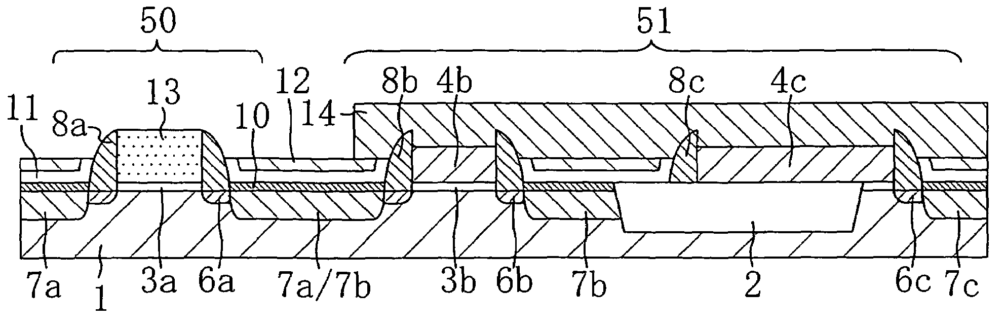
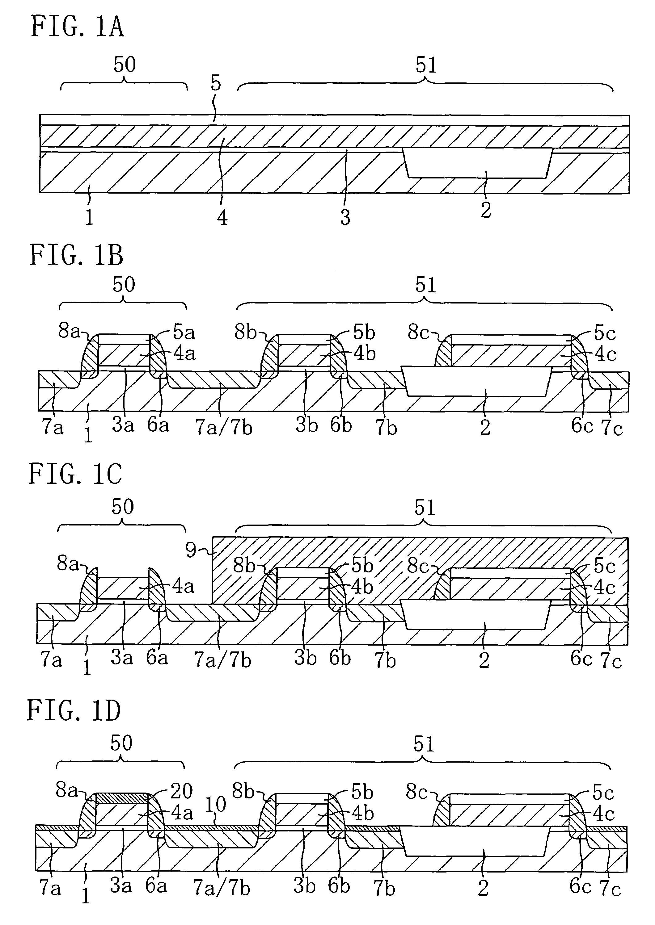
[0027]FIGS. 1A through 1D are cross-sectional views illustrating a fabrication method for a semiconductor device according to the first embodiment of the present invention. “Dummy gate electrodes” herein represent gate electrodes of a semiconductor device that are not concerned with circuit operation. As previously described, dummy gate electrodes are formed to finish gate electrodes as designed or to make the top surface of an interlayer dielectric uniform in planarization of the interlayer dielectric. When dummy gate electrodes are formed to finish gate electrodes as designed, they each often have a gate length of 10 μm or less. When dummy gate electrodes are formed to make the thickness of an interlayer dielectric uniform, they each often have a gate length of 10 μm. In this embodiment, a description will be given of a fabrication method for a semiconductor device including a MIS tr...

embodiment 2

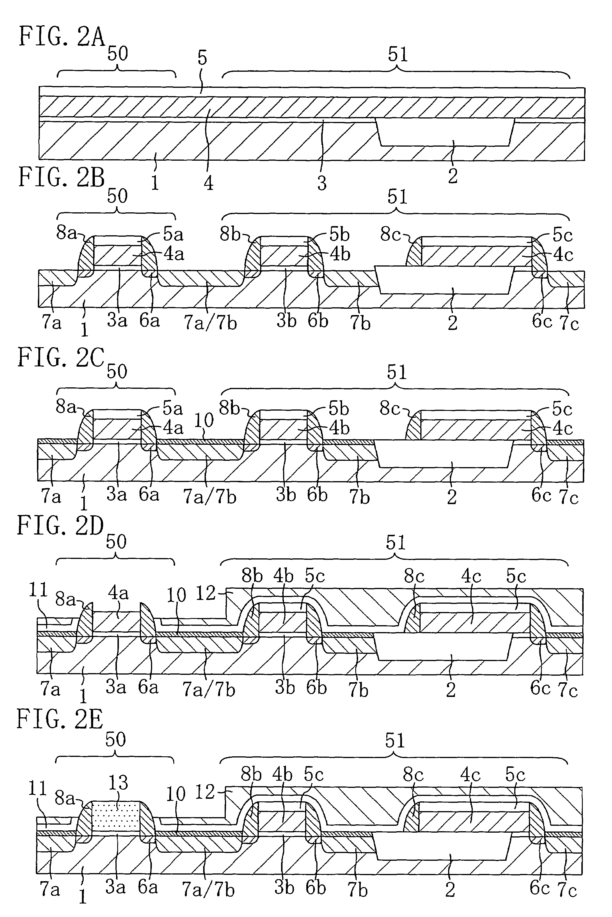
[0041]FIGS. 2A through 2E are cross-sectional views illustrating a fabrication method for a semiconductor device according to a second embodiment of the present invention. In these figures, the same components as those of the semiconductor device of the first embodiment are denoted by the same reference numerals, and thus a description of the same components will be simplified.

[0042]First, in the process step illustrated in FIG. 2A, like the process step illustrated in FIG. 1A of the first embodiment, an isolation region 2 is selectively formed in a semiconductor substrate 1. As a result, active regions are formed in the semiconductor substrate 1 so as to be surrounded by the isolation region 2. Subsequently, a 2-nm-thick first insulating film 3 and a 100-nm-thick polysilicon film 4 are deposited on the semiconductor substrate 1. Thereafter, a 20-nm-thick second insulating film 5 is deposited on the top surface of the polysilicon film 4.

[0043]Next, in the process step illustrated in...

embodiment 3

[0055]Another method for selectively siliciding only a gate electrode formed on an element formation region will be described in a third embodiment of the present invention.

[0056]FIGS. 3A through 3E are cross-sectional views illustrating a fabrication method for a semiconductor device according to the third embodiment of the present invention. In these figures, the same components as those of the semiconductor device of each of the first and second embodiments are denoted by the same reference numerals, and thus a description of the same components will be simplified.

[0057]First, in the process step illustrated in FIG. 3A, like the process step illustrated in FIG. 1A of the first embodiment, an isolation region 2 is selectively formed in a semiconductor substrate 1. As a result, active regions are formed in the semiconductor substrate 1 so as to be surrounded by the isolation region 2. Subsequently, for example, a 2-nm-thick first insulating film 3 and a 100-nm-thick polysilicon fil...


PUM


Abstract

The following steps are carried out: forming a gate electrode on a semiconductor substrate with a gate insulating film interposed therebetween, forming a dummy gate electrode on the semiconductor substrate with a dummy gate insulating film interposed therebetween and forming another dummy gate electrode on the semiconductor substrate with an insulating film for isolation interposed therebetween; forming a metal film on the semiconductor while exposing the gate electrode and covering the dummy gate electrodes; and subjecting the semiconductor substrate to heat treatment and thus siliciding at least an upper part of the gate electrode. Since the gate electrode is silicided and the dummy gate electrodes are non-silicided, this restrains a short circuit from being caused between the gate electrode and adjacent one of the dummy gate electrodes.

Description

BACKGROUND OF THE INVENTION[0001](1) Field of the Invention[0002]The present invention relates to semiconductor devices including gate electrodes and dummy gate electrodes and methods for fabricating the same.[0003](2) Description of Related Art[0004]In recent years, with an increasing degree of integration of semiconductor integrated circuits and an increasing operating speed thereof, increasing significance has been attached to control over the dimensions of gate electrodes of MIS transistors which significantly influence the characteristics of semiconductor integrated circuits. Meanwhile, a part of a semiconductor integrated circuit in which MIS transistors densely exist and a part thereof in which MIS transistors sparsely exist are both necessarily mixed in the semiconductor integrated circuit. Such variations in the density of MIS transistors formed in a semiconductor integrated circuit have an influence on processes for processing gate electrodes of MIS transistors, such as a ...

Claims


Application Information

Patent Timeline
Patent Type & Authority Patents(United States)
IPC IPC(8): H01L29/78
CPCH01L21/823437H01L21/823443H01L21/82345H01L27/0207H01L29/665
Inventor AIDA, KAZUHIKOHIRASE, JUNJIOGAWA, HISASHIKUDO, CHIAKI
Owner GK BRIDGE 1
Why Eureka
Try Eureka