Methods for generating a user interface for timing budget analysis of integrated circuit designs

a technology for integrated circuits and user interfaces, applied in software simulation/interpretation/emulation, instruments, program control, etc., can solve the problems of complex and time-consuming task of designing these integrated circuits, complicating the evaluation of the overall circuit design, and achieving better integrated circuit design. , the effect of improving the semiconductor manufacturing of the integrated circui

Active Publication Date: 2014-06-03
CADENCE DESIGN SYST INC
View PDF7 Cites 5 Cited by
  • Summary
  • Abstract
  • Description
  • Claims
  • Application Information

AI Technical Summary

Benefits of technology

[0008]A timing budgeting process for designing an integrated circuit is disclosed that provides a timing budget graphical user interface (GUI). The timing budget graphical user interface (GUI) may include one or more windows of information that is graphically displayed to a user. Generally for one or more selected paths (which may be automatically selected by a path category), the timing budgeting GUI graphically displays timing delay calculations (e.g., slack calculations) with a color coded cumulative histogram of rectangles and lines next to hierarchy information and a color coded cumulative histogram of timing budget information allocated to the hierarchy of the integrated circuit design, so that a visual comparison may be readily made. If the graphical objects of the timing budgeting GUI indicate that the timing delays are over budget, the timing budgets may be adjusted and / or the integrated circuit redesigned so that the timing delays better meet the timing budgets of the integrated circuit design. In either case with a better integrated circuit design, the semiconductor manufacturing of the integrated circuit may be improved.

Problems solved by technology

Integrated circuits have become larger and more complex to provide additional functionality and / or improved performance.
The task of designing these integrated circuits is also very complex and time consuming, involving synthesizing, analyzing and optimizing many circuit parameters.
However, dividing up an integrated circuit design into multiple blocks and hierarchical levels can complicate the evaluation of the overall circuit design.
Timing budgets for signal paths are usually automatically generated in early design stages when the integrated circuit design may be incomplete or have errors so that generated timing budgets may require manual correction and analysis.
However, this time budgeting data is usually represented by one or more simple text files that have large file sizes (e.g., gigabyte size), making it difficult to timely analyze.
Moreover if a user changes one block constraint, it is often very difficult to propagate changes to other blocks of the integrated circuit design using text files.

Method used


Image

  • Methods for generating a user interface for timing budget analysis of integrated circuit designs
  • Methods for generating a user interface for timing budget analysis of integrated circuit designs
  • Methods for generating a user interface for timing budget analysis of integrated circuit designs

Examples


Embodiment Construction

[0018]In the following detailed description of the embodiments of the invention, numerous specific details are set forth in order to provide a thorough understanding of the present invention. However, it will be obvious to one skilled in the art that the embodiments of the invention may be practiced without these specific details. In other instances well known methods, procedures, components, and circuits have not been described in detail so as not to unnecessarily obscure aspects of the embodiments of the invention.

Introduction

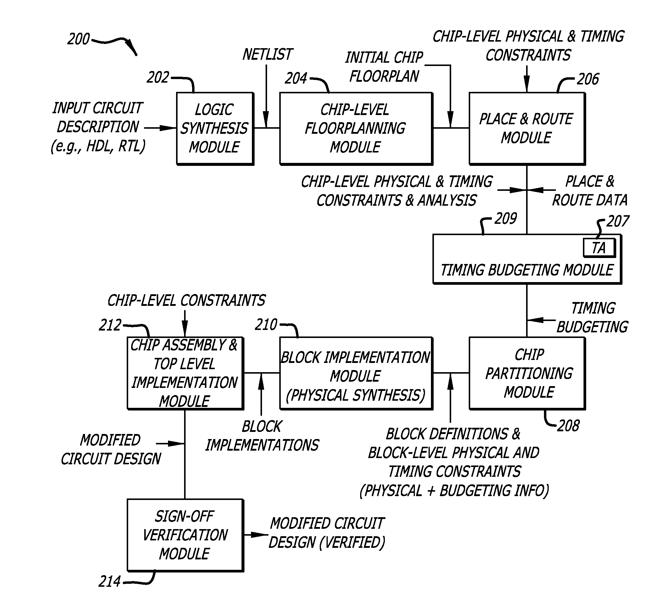
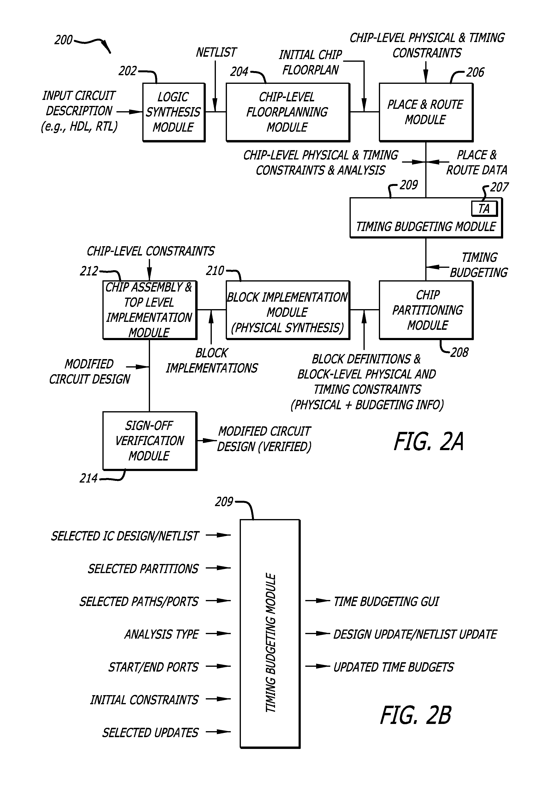
[0019]The embodiments of the invention facilitate budgeting of signal timing between functional blocks or modules of an integrated circuit design which may be referred to as timing budgeting. U.S. patent application Ser. No. 11 / 621,915, entitled SYSTEM AND METHOD OF GENERATING HIERARCHICAL BLOCK-LEVEL TIMING CONSTRAINTS FROM CHIP-LEVEL TIMING CONSTRAINTS filed by Levitsky et al. on Jan. 10, 2007, hereby incorporated by reference, describes embodiments that ge...


PUM


Abstract

In one embodiment of the invention, a method includes reading an automatically generated timing budgeting file, including timing budget information for a plurality of partitions of an integrated circuit design; graphically displaying a time budgeting debug window on a display device; and graphically displaying a timing budget analyzer window on the display device in response to selection of a selected signal path in a path list window pane. The timing budget analyzer window graphically displays timing budgets and timing delays of a selected path for visual comparison. The time budgeting debug window includes a button with a path category menu to display one or more signal paths meeting a selected path category, and a path list window pane to display a list of one or more signal paths through one or more ports of the plurality of partitions in response to the selected path category in the path category menu.

Description

CROSS-REFERENCE TO RELATED APPLICATIONS[0001]This non-provisional United States (U.S.) patent application is a divisional and claims the benefit of U.S. patent application Ser. No. 12 / 437,096 filed on May 7, 2009 by inventors Vivek Bhardwaj, et al., entitled USER INTERFACE FOR TIMING BUDGET ANALYSIS OF INTEGRATED CIRCUIT DESIGNS. U.S. patent application Ser. No. 12 / 437,096 claims the benefit and is a non-provisional of U.S. Provisional Patent Application No. 61 / 164,860 entitled USER INTERFACE FOR TIMING BUDGET ANALYSIS OF INTEGRATED CIRCUIT DESIGNS filed on Mar. 30, 2009 by inventors Vivek Bhardwaj et al.FIELD OF THE INVENTION[0002]This invention relates to user interfaces for evaluating timing constraints of integrated circuit designs.BACKGROUND OF THE INVENTION[0003]Integrated circuits have become larger and more complex to provide additional functionality and / or improved performance. The task of designing these integrated circuits is also very complex and time consuming, involvin...

Claims


Application Information

Patent Timeline
Patent Type & Authority Patents(United States)
IPC IPC(8): G06F17/50G06F9/455
CPCG06F17/5036G06F2217/84G06F30/367G06F2119/12
Inventor BHARDWAJ, VIVEKSEROPIAN, DIDIERLEVITSKY, OLEG
Owner CADENCE DESIGN SYST INC
Why Eureka
Try Eureka