Embedded wafer level ball grid array bar systems and methods

a grid array and wafer technology, applied in the field of integrated circuit packaging, can solve the problems of reducing the package size, limiting the ball pitch, and physically impossible distribution of solder balls on the semiconductor die itself, so as to achieve easy adjustment, easy change or variation, and easy variation

Inactive Publication Date: 2014-08-05
STMICROELECTRONICS PTE LTD
View PDF4 Cites 2 Cited by
  • Summary
  • Abstract
  • Description
  • Claims
  • Application Information

AI Technical Summary

Benefits of technology

[0009]According to principles as explained herein, stacked top and bottom semiconductor packages forming a PoP package are physically and electrically coupled using a conductive material surrounded by a reconstituted wafer. The reconstituted wafer is first formed about a plurality of dies then a number of voids are formed within the reconstituted wafer. The voids are filled with a conductive material to form a bar having at least one, but often more, individual conductive material filled voids surrounded by the reconstituted wafer. The number of conductors within the bar can be easily adjusted by forming and filling a greater or lesser number of voids within the reconstituted wafer. Similarly, the pattern formed by the conductive material filled voids or conductors in the bar can be easily changed or varied to accommodate the stacking of semiconductor packages having different sizes, shapes, physical configurations, conductor counts, contact pad arrangements, etc. within the PoP package. Additionally, one or more physical dimensions of the bar, such as the height of the bar, may be easily varied by adjusting the thickness or finishing of the reconstituted wafer surrounding the conductive material filled voids or conductors to accommodate the gap between the PoPt and PoPb packages forming the PoP package.

Problems solved by technology

The reduced package size may render the distribution of solder balls on the semiconductor die itself physically impossible—for example where the resultant contact pad pitch would be less than the diameter of the solder balls used to in the ball grid array.
Larger diameter solder balls are used to span the increased distance between the PoPt package and the fan out area of the PoPb package however, the use of larger solder balls to attach the PoPt package to the PoPb package effectively decreases the solder ball density (or, alternatively, limits the ball pitch) achievable on the PoPt package ball grid array.
Thermal cycling the PoP package can cause fatigue or stress cracks to form in the solder connections linking the various packages forming the PoP or between the PoP package and the circuit board to which the package is attached.
The use of larger solder balls to span the distance between PoPt and PoPb packages exacerbates the issues by increasing the forces exerted on the solder connections.

Method used


Image

  • Embedded wafer level ball grid array bar systems and methods
  • Embedded wafer level ball grid array bar systems and methods
  • Embedded wafer level ball grid array bar systems and methods

Examples


Embodiment Construction

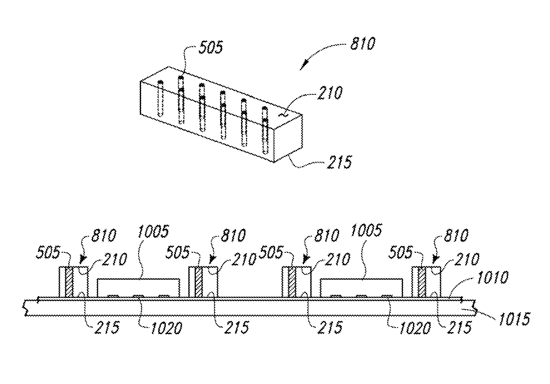
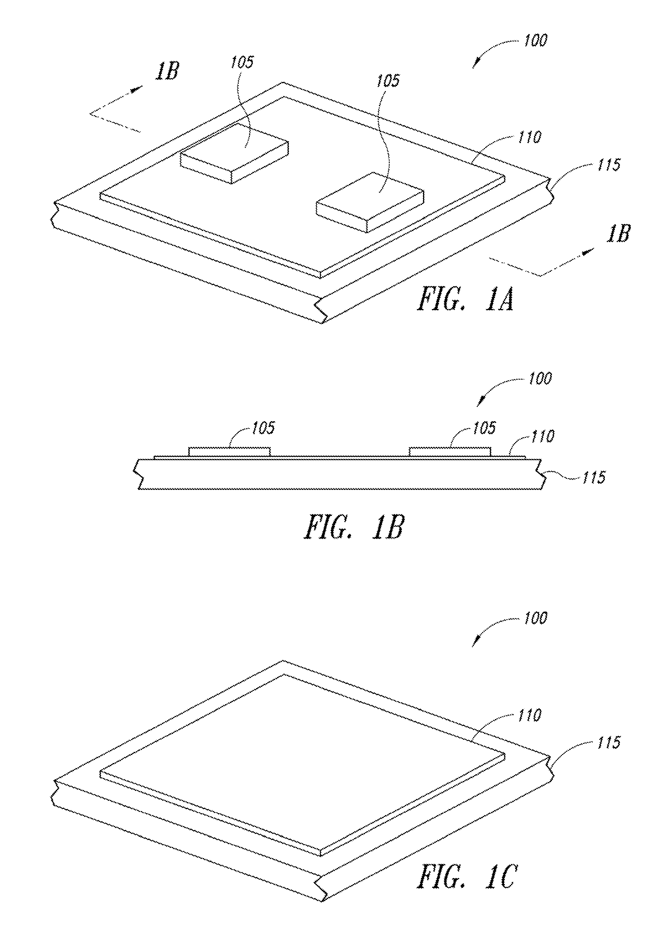
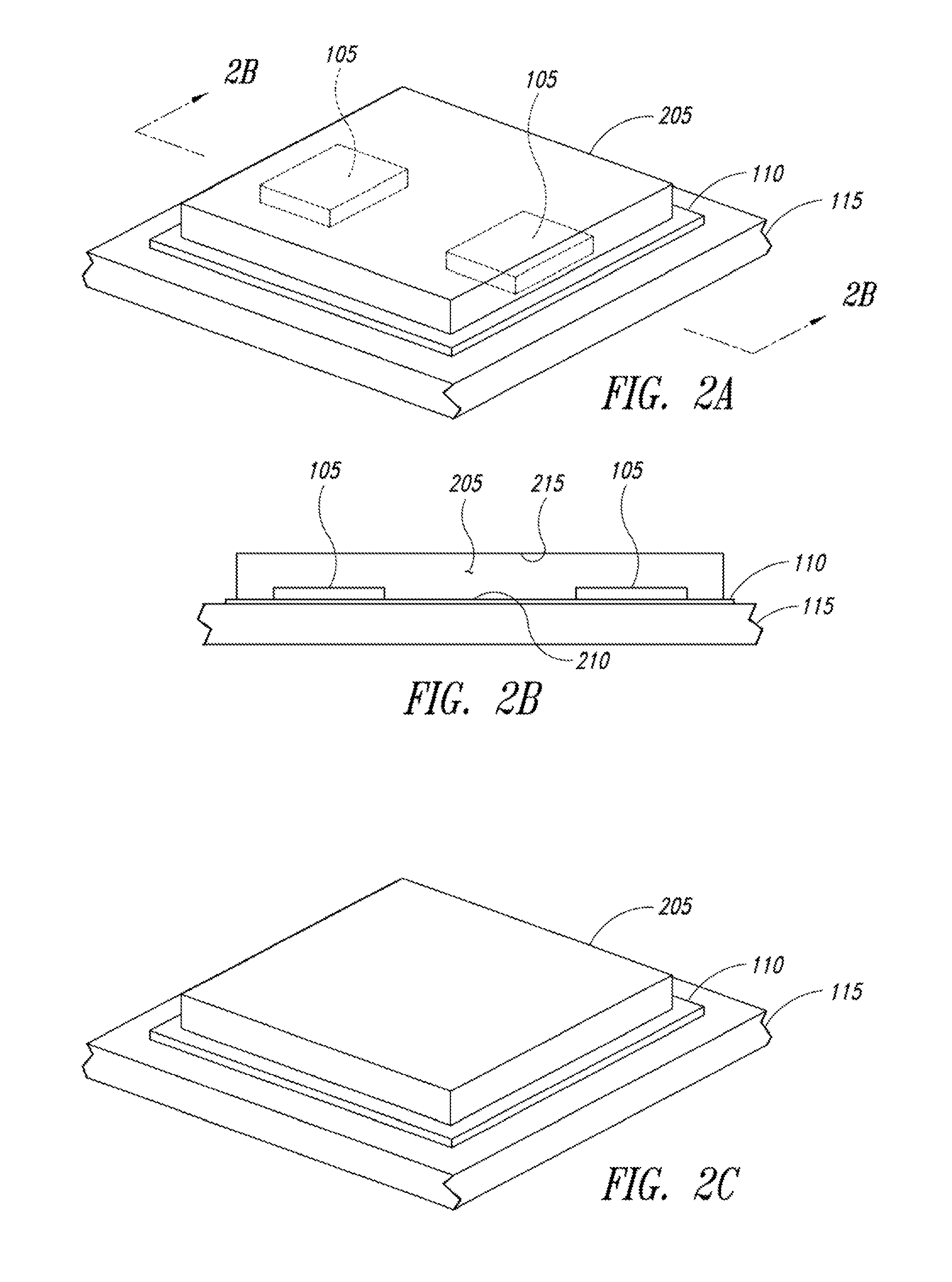
[0027]In the following description, certain specific details are set forth in order to provide a thorough understanding of various disclosed embodiments. However, one skilled in the relevant art will recognize that embodiments may be practiced without one or more of these specific details, or with other methods, components, materials, etc.

[0028]Unless the context requires otherwise, throughout the specification and claims which follow, the word “comprise” and variations thereof, such as “comprises” and “comprising” are to be construed in an open, inclusive sense, that is, as “including, but not limited to.”

[0029]Reference throughout this specification to “one embodiment” or “an embodiment” means that a particular feature, structure, or characteristic described in connection with the embodiment is included in at least one embodiment. Thus, the appearances of the phrases “in one embodiment” or “in an embodiment” in various places throughout this specification are not necessarily all r...


PUM


Abstract

A bar formed from a reconstituted wafer and containing one or more conductive material filled voids is used to electrically and physically connect the top and bottom packages in a package-on-package (PoP) package. The bar is disposed in the fan out area of the lower package forming the PoP package.

Description

BACKGROUND[0001]1. Technical Field[0002]This disclosure generally relates to packaging of integrated circuits and particularly relates to conductive bar systems useful in the production of package-on-package (PoP) semiconductor packages.[0003]2. Description of the Related Art[0004]Ongoing demand for smaller electronic devices has pressured manufacturers of such devices to increase the component density and reduce the component size wherever possible within the device. Integrated circuit manufacturers have responded by increasing the use of chip scale packaging and wafer level packaging techniques to minimize the footprint of the integrated circuit package, at times reducing the package to a size approaching the size of the semiconductor die itself through the use of direct surface mountable ball grid arrays and flip chip configurations.[0005]The drive to reduce size is not without consequences, however. The reduced package size may render the distribution of solder balls on the semi...

Claims


Application Information

Patent Timeline
Patent Type & Authority Patents(United States)
IPC IPC(8): H01L21/44
CPCH01L21/565H01L21/561H01L25/105H01L23/49838H01L24/19H01L2225/1041H01L21/568H01L2224/12105H01L2224/96H01L2225/1058H01L23/3128H01L24/96H01L2225/1023H05K2203/025H05K3/4623H05K1/142H05K1/188H05K1/0373H05K1/186H01L2924/181H01L2924/12042H01L2924/15311H01L2224/03H01L2924/00
Inventor RAMASAMY, ANANDANJIN, YONGGANGLIU, YUN
Owner STMICROELECTRONICS PTE LTD
Why Eureka
Try Eureka