Semiconductor device

a technology of semiconductor devices and semiconductors, applied in the direction of semiconductor devices, basic electric elements, electrical appliances, etc., can solve the problems of reducing the reliability of semiconductor devices including transistors, affecting the operation of semiconductor devices, and affecting the reliability of semiconductor devices. achieve the effect of stable electrical characteristics

Inactive Publication Date: 2014-08-05
SEMICON ENERGY LAB CO LTD
View PDF172 Cites 43 Cited by
  • Summary
  • Abstract
  • Description
  • Claims
  • Application Information

AI Technical Summary

Benefits of technology

[0006]A transistor including an oxide semiconductor film operates faster (it can also be said that the field effect mobility is higher) than a transistor including an amorphous silicon film and is manufactured more easily than a transistor including a polycrystalline silicon film.

Problems solved by technology

However, some problems of the transistor including an oxide semiconductor film have been pointed out.
One of the problems is unstable electrical characteristics of the transistor.
Specifically, a problem that the threshold voltage of the transistor is negatively shifted by a bias-temperature stress test (also referred to as a BT stress test) or irradiation with visible light or ultraviolet light, so that the transistor tends to be normally on has been pointed out.
When the oxide semiconductor film is amorphous, for example, the bonding state of metal atoms and oxygen atoms in the oxide semiconductor film is not ordered; thus, oxygen deficiency is likely to be generated.
Such a change can cause variations in the electrical characteristics of a transistor, which leads to a reduction in reliability of a semiconductor device including the transistor.
However, before the formation of the oxide semiconductor film (in other words, before the oxygen supply to the oxide semiconductor film), heat treatment or the like in a manufacturing process might cause oxygen to be released from the oxide film or the like formed in the vicinity of the oxide semiconductor film, which would result in insufficient supply of oxygen to the oxide semiconductor film.

Method used


Image

  • Semiconductor device
  • Semiconductor device
  • Semiconductor device

Examples


embodiment 1

[0070]In this embodiment, one embodiment of a semiconductor device and a method for manufacturing the semiconductor device will be described with reference to FIGS. 1A to 1C, FIGS. 2A to 2D, and FIGS. 3A to 3D.

example 1

Structural Example 1 of Semiconductor Device

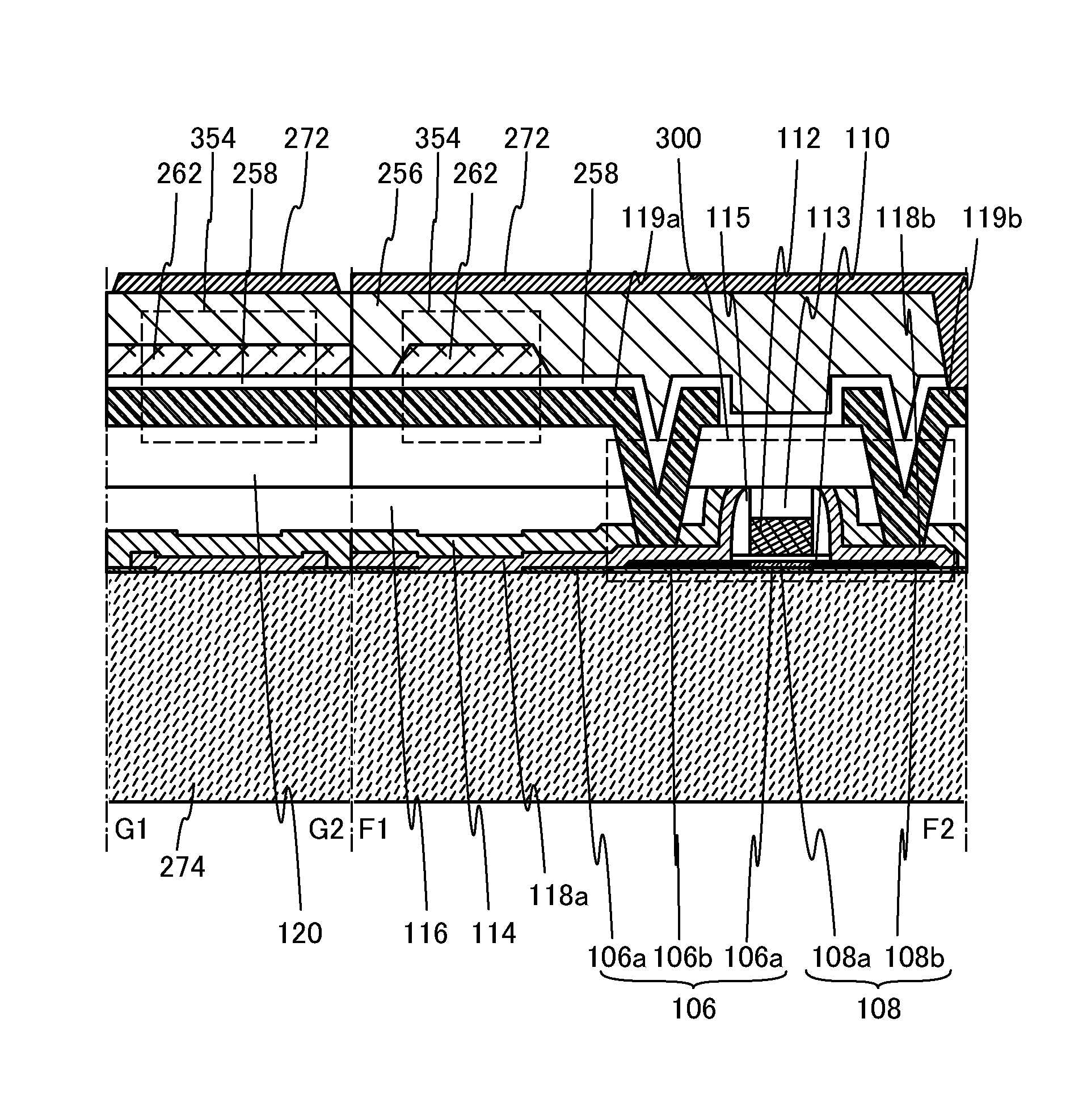
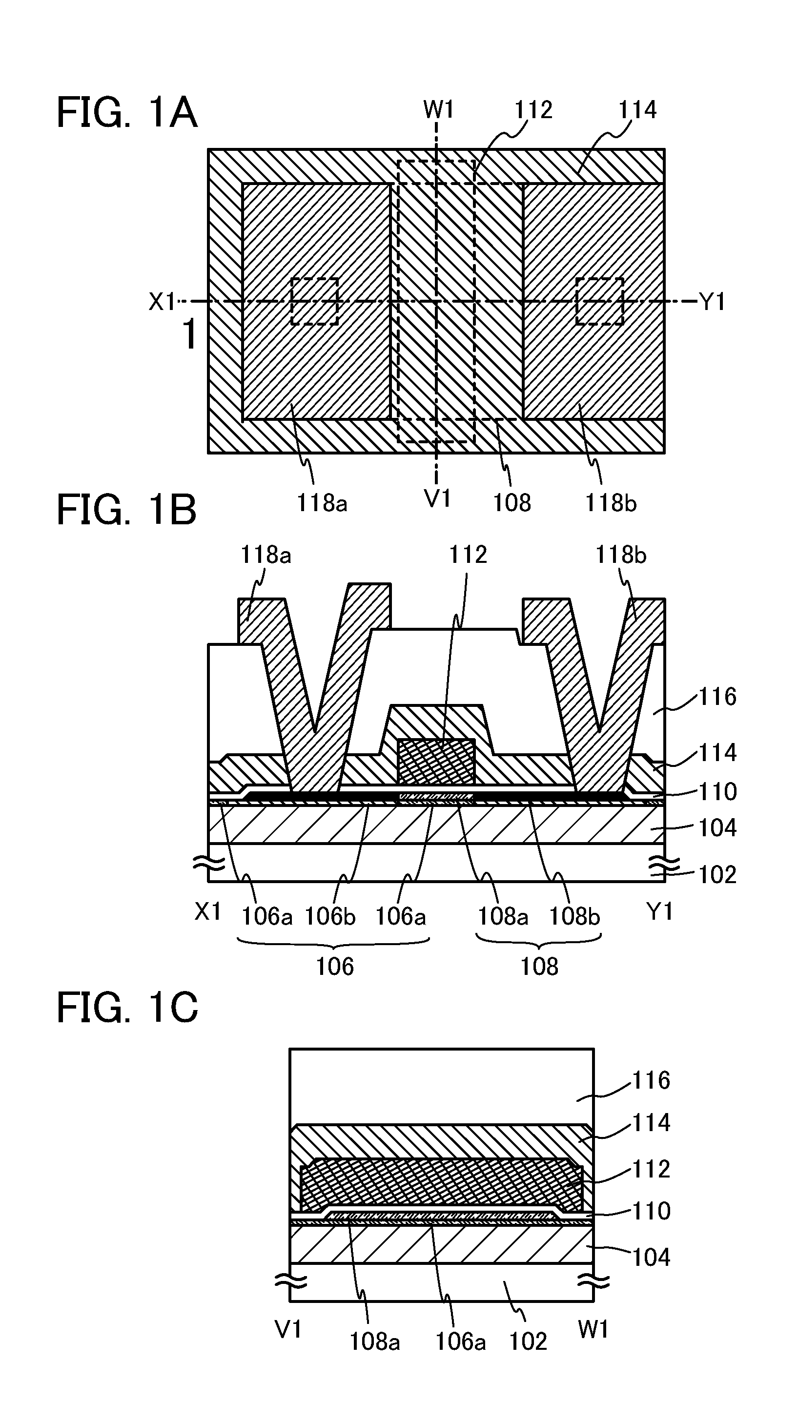
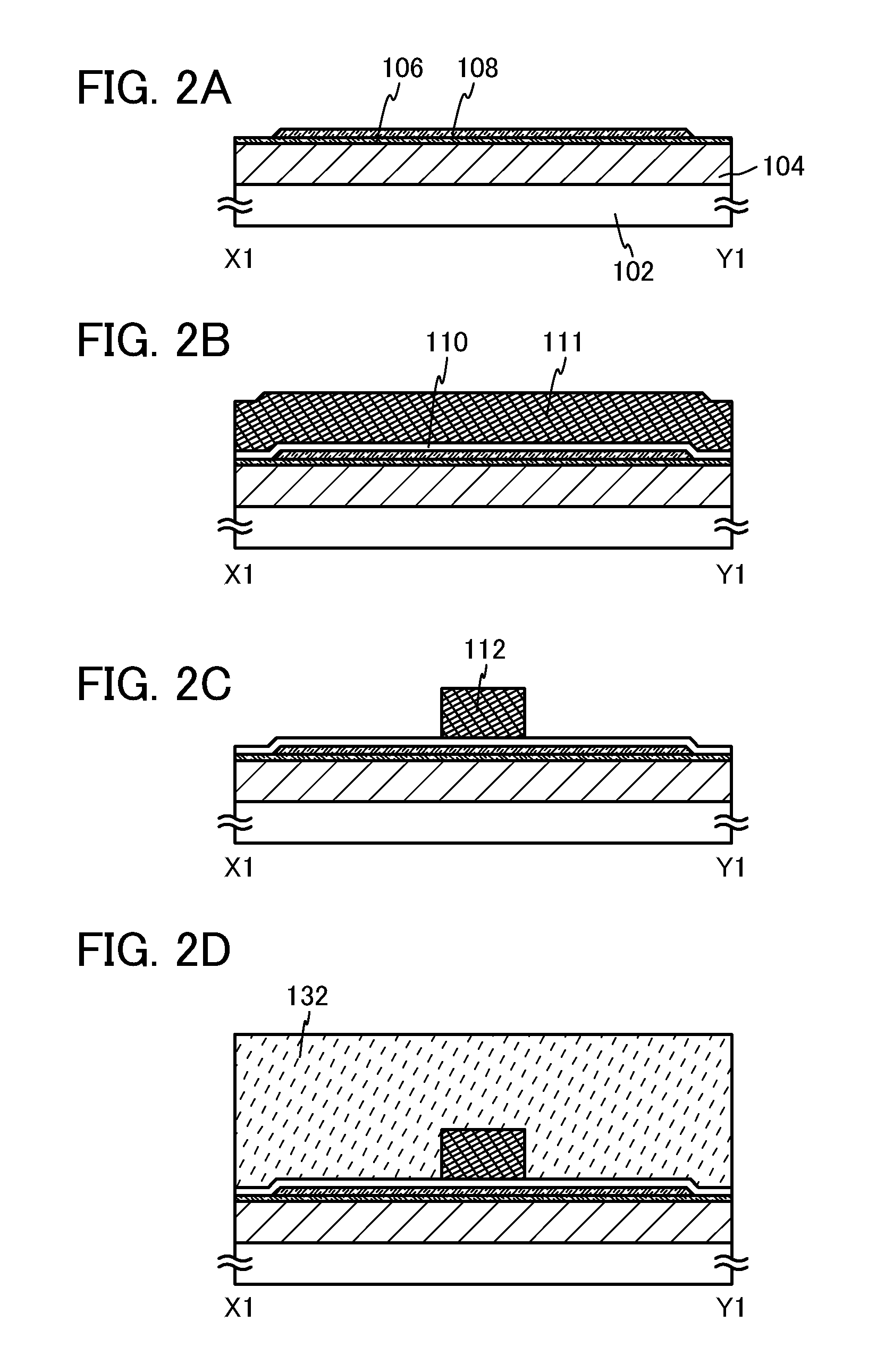
[0071]A plan view and cross-sectional views of a top-gate transistor as an example of the semiconductor device are illustrated in FIGS. 1A to 1C. FIG. 1A is the plan view, FIG. 1B corresponds to a cross-sectional view taken along line X1-Y1 in FIG. 1A, and FIG. 1C corresponds to a cross-sectional view taken along line V1-W1 in FIG. 1A. Note that in FIG. 1A, some components of the semiconductor device (e.g., a gate insulating film 110) are omitted for simplicity.

[0072]The semiconductor device illustrated in FIGS. 1A to 1C includes an oxide film 104; a first oxide semiconductor film 106 formed over the oxide film 104; a second oxide semiconductor film 108 formed over the first oxide semiconductor film 106; the gate insulating film 110 formed over the second oxide semiconductor film 108; and a gate electrode 112 which is in contact with the gate insulating film 110 and formed in a region overlapping with the second oxide semiconductor film 10...

embodiment 2

[0189]In this embodiment, a modification example of the semiconductor device in Embodiment 1 and a method for manufacturing a semiconductor device, which is different from that in Embodiment 1, will be described with reference to FIGS. 4A to 4C, FIGS. 5A to 5D, and FIGS. 6A to 6C. Note that portions similar to those in FIGS. 1A to 1C, FIGS. 2A to 2D, and FIGS. 3A to 3D are denoted by the same reference numerals, and description thereof is omitted. In addition, detailed description of the same portions is not repeated, either.


PUM


Abstract

Provided is a transistor which includes an oxide semiconductor film and has stable electrical characteristics. In the transistor, over an oxide film which can release oxygen by being heated, a first oxide semiconductor film which can suppress oxygen release at least from the oxide film is formed. Over the first oxide semiconductor film, a second oxide semiconductor film is formed. With such a structure in which the oxide semiconductor films are stacked, the oxygen release from the oxide film can be suppressed at the time of the formation of the second oxide semiconductor film, and oxygen can be released from the oxide film in later-performed heat treatment. Thus, oxygen can pass through the first oxide semiconductor film to be favorably supplied to the second oxide semiconductor film. Oxygen supplied to the second oxide semiconductor film can suppress the generation of oxygen deficiency, resulting in stable electrical characteristics.

Description

TECHNICAL FIELD[0001]The present invention relates to a semiconductor device including an oxide semiconductor.[0002]In this specification, a semiconductor device refers to a device which can function by utilizing semiconductor characteristics; a transistor, an electro-optical device, a semiconductor circuit, and an electronic device are all included in the category of the semiconductor device.BACKGROUND ART[0003]A technique by which transistors are formed using semiconductor thin films formed over a substrate having an insulating surface has been attracting attention. The transistor is applied to a wide range of electronic devices such as an integrated circuit (IC) or an image display device (display device). A silicon-based semiconductor material is widely known as a material for a semiconductor thin film applicable to a transistor. As another material, an oxide semiconductor has been attracting attention.[0004]For example, a transistor including an amorphous oxide semiconductor fi...

Claims


Application Information

Patent Timeline
Patent Type & Authority Patents(United States)
IPC IPC(8): H01L29/12
CPCH01L29/78693H01L29/7869H01L29/78696H01L29/045H01L29/24
Inventor YAMAZAKI, SHUNPEI
Owner SEMICON ENERGY LAB CO LTD
Why Eureka
Try Eureka